LC75878W 데이터 시트보기 (PDF) - ON Semiconductor
부품명
상세내역
제조사
LC75878W Datasheet PDF : 36 Pages
| |||
Control Data Functions
LC75878W
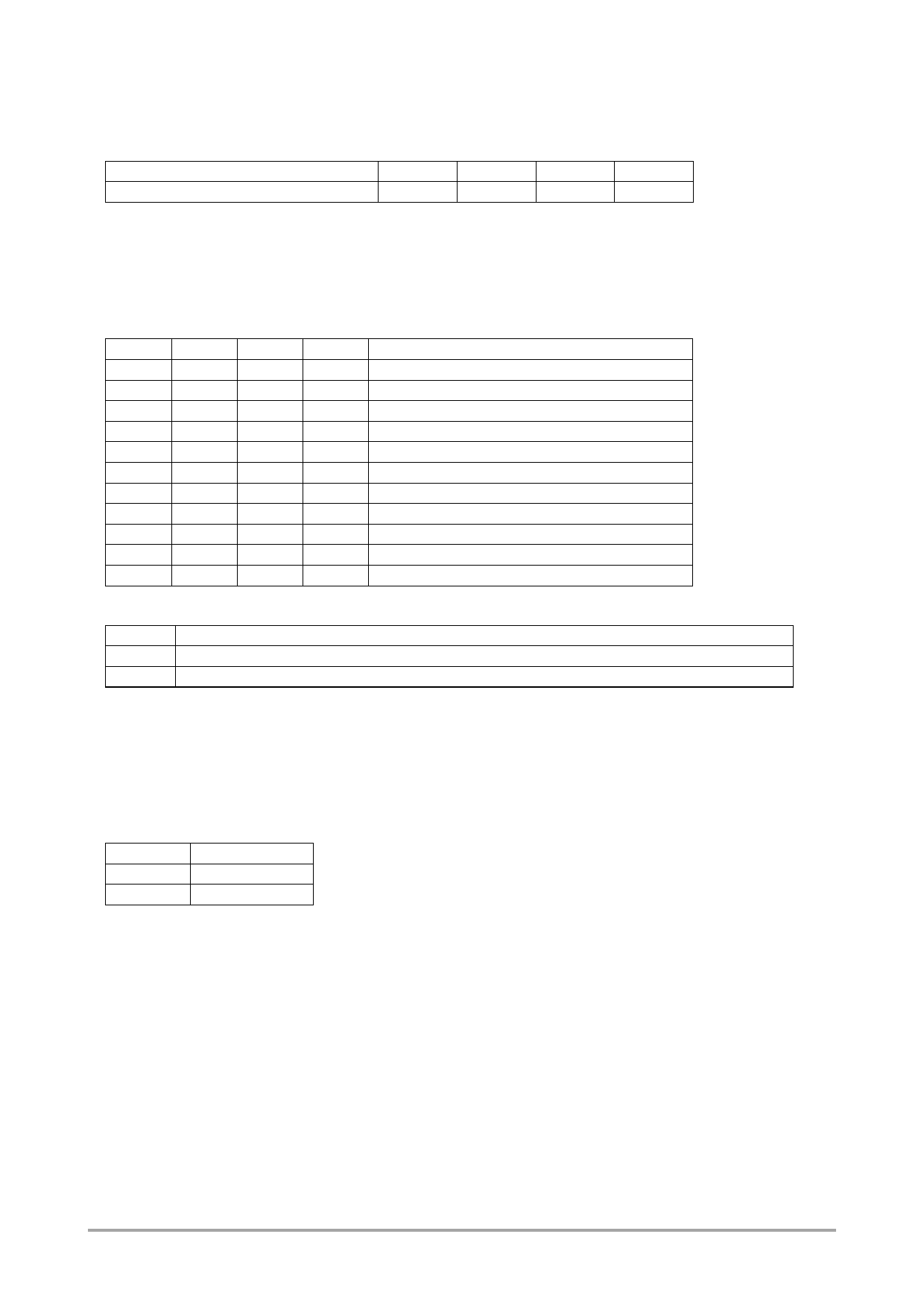
1. PC1 to PC4: General-purpose output port state setting data
These control data bits set the states of the general-purpose output ports P1 to P4.
Output pin
P1
P2
P3
P4
General-purpose output port state setting data
PC1
PC2
PC3
PC4
For example, if PC1 and PC2 are set to 1, and PC3 and PC4 are set to 0, then the output pins P1 and P2 will output
high levels (VDD) and the output pins P3 and P4 will output low levels (VSS).
2. CT0 to CT3, CTC: Display contrast setting data
These control data bits set the display contrast.
CT0 to CT3: Display contrast setting (11 steps)
CT0
CT1
CT2
CT3
LCD drive 4/4 bias voltage supply VLCD0 level
0
0
0
0
0.94VLCD=VLCD-(0.03VLCD2)
1
0
0
0
0.91VLCD=VLCD-(0.03VLCD3)
0
1
0
0
0.88VLCD=VLCD-(0.03VLCD4)
1
1
0
0
0.85VLCD=VLCD-(0.03VLCD5)
0
0
1
0
0.82VLCD=VLCD-(0.03VLCD6)
1
0
1
0
0.79VLCD=VLCD-(0.03VLCD7)
0
1
1
0
0.76VLCD=VLCD-(0.03VLCD8)
1
1
1
0
0.73VLCD=VLCD-(0.03VLCD9)
0
0
0
1
0.70VLCD=VLCD-(0.03VLCD10)
1
0
0
1
0.67VLCD=VLCD-(0.03VLCD11)
0
1
0
1
0.64VLCD=VLCD-(0.03VLCD12)
CTC: Display contrast adjustment circuit state setting
CTC
Display contrast adjustment circuit state
0
The display contrast adjustment circuit is disabled, and the VLCD0 pin level is forced to the VLCD level.
1
The display contrast adjustment circuit operates and the display contrast is adjusted.
Note that although the display contrast can be adjusted by operating the built-in display contrast adjustment circuit, it
is also possible to apply fine adjustments to the contrast by connecting an external variable resistor to the VLCD4 pin
and modifying the VLCD4 pin voltage. However, the following conditions must be met: (VLCD0 – VLCD4) 4.5 V,
and 1.5 V VLCD4 0 V.
3. SC: Segment on/off control data
This control data bit controls the on/off state of the segments.
SC
Display state
0
On
1
Off
However, note that when the segments are turned off by setting SC to 1, the segments are turned off by outputting
segment off waveforms from the segment output pins.
www.onsemi.com
19
Share Link: 