83C196NH 데이터 시트보기 (PDF) - Intel
부품명
상세내역
제조사
83C196NH Datasheet PDF : 41 Pages
| |||
8XC196MH INDUSTRIAL MOTOR CONTROL CHMOS MICROCONTROLLER
®
DC CHARACTERISTICS
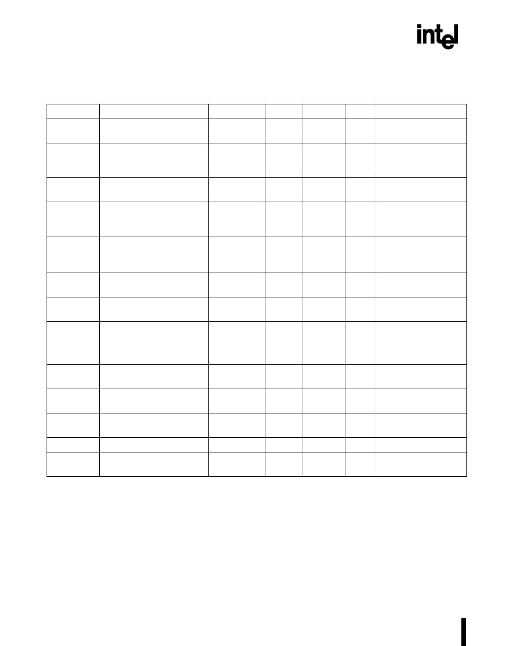
Table 8. DC Characteristics over Specified Operating Conditions
Symbol
Parameter
Min
Typ (4) Max Units Test Conditions
VIL
Input Low Voltage
(standard inputs (1))
– 0.5
0.3 VCC
V
VIL1
Input Low Voltage
– 0.5
(RESET#, ports 3, 4, and
5)
0.8
V
VIH
Input High Voltage
0.7 VCC
(standard inputs (1))
VCC + 0.5 V
VIH1
Input High Voltage
0.2 VCC + 1.0
(RESET#, ports 3, 4, and
5)
VCC + 0.5 V
VOL
Output Low Voltage
(RESET#, ports 1, 2, 5,
P6.6, P6.7, and XTAL2)
VOL1
Output Low Voltage (ports
3, 4)
0.3
0.45
1.5
1.0
V IOL = 200 µA
V IOL = 3.2 mA
V IOL = 7.0 mA
V IOL = 7 mA
VOL2
Output Low Voltage
(P6.5:0)
0.45
V IOL = 10 mA
VOH
Output High Voltage
VCC – 0.3
(output pins and I/O
VCC – 0.7
configured as push/pull
VCC – 1.5
outputs)
V IOH = – 200 µA
V IOH = – 3.2 mA
V IOH = – 7.0 mA
VTH+ – VTH– Hysteresis voltage width
0.2
V
on RESET# pin
ILI
Input Leakage Current
(standard inputs (1))
± 10
µA VSS < VIN < VCC – 0.3V
ILI1
Input Leakage Current
(port 0 – A/D inputs)
±3
µA VSS < VIN < VREF
IIH
Input High Current (NMI)
IIL
Input Low Current (port 2,
except P2.6)
300
− 70
µA VIN = 0.7 VCC
µA VIN = 0.3 VCC
NOTES:
1. Standard input pins include XTAL1, EA#, and Ports 1 and 2 when configured as inputs.
2. Maximum current that an external device must sink to ensure test mode entry.
3. Violating these specifications during reset may cause the device to enter test modes.
4. Typical values are based on a limited number of samples and are not guaranteed. Operating conditions
for typical values are room temperature and VREF = VCC = 5.5 V.
5. Testing is performed down to 8 MHz, although the device is static by design and will typically operate
below 1 Hz.
6. All voltages are referenced relative to VSS. When used, VSS refers to the device pin.
7. Table 9 lists the total current limits during normal (non-transient conditions). The total current listed is the
sum of the pins listed for each specification value.
20
Share Link: 