LC5824 데이터 시트보기 (PDF) - SANYO -> Panasonic
부품명
상세내역
제조사
LC5824 Datasheet PDF : 24 Pages
| |||
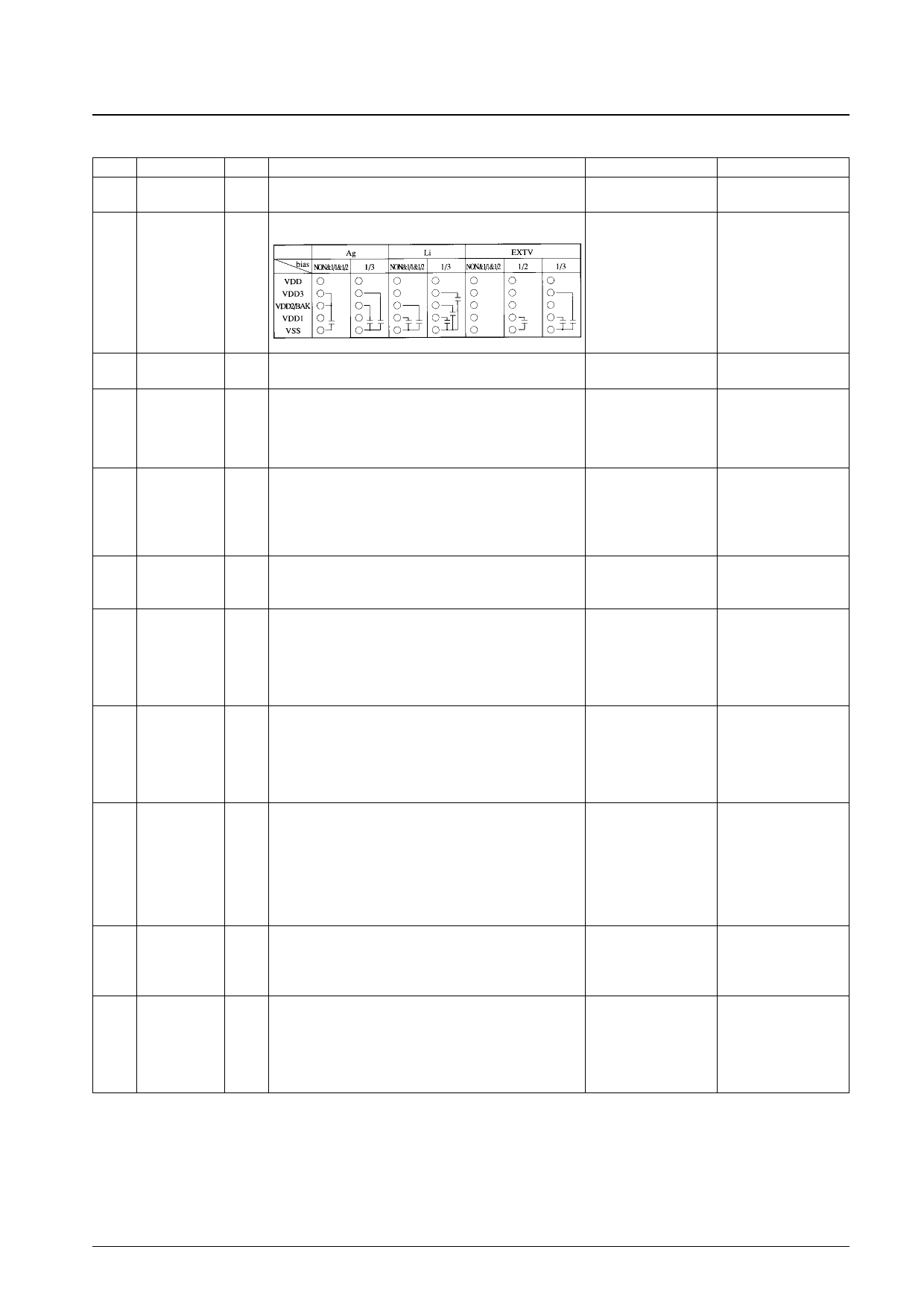
Pin Functions
Pin No.
Pin
24
VDD
25
VSS
30
VDD1
29
VDD2/BAK
28
VDD3
LC5824, LC5823, LC5822
I/O
Function
— Power supply
—
LCD drive power supply
—
Power supply
specifications
Pin
—
—
Options
• Ag specifications
• Li specifications
• EXT-V specifications
Status at reset
42
CUP1
— Connections of the LCD power supply step-up (step-down)
43
CUP2
— capacitors
System clock oscillator connections
26
27
CFIN
CFOUT
Input
Output
• Ceramic element connections (CF specifications)
• RC component connections (RC specifications)
*: This oscillator circuit is stopped when a STOP or SLOW
• CF specifications
• RC specifications
• Unused
instruction is executed.
Used for reference counting (clock specifications, LCD
alternation frequency) and as the system clock.
• 32-kHz specifications
23
XTIN
Input • 32-kHz crystal oscillator
• 65-kHz specifications
22
XTOUT
Output • 65-kHz crystal oscillator
• 38-kHz specifications
*: This oscillator circuit is stopped when a STOP instruction is • Unused
executed.
Used for the phase compensation capacitor connected between
—
XC
— this pin and XTOUT and XTIN. This pin is only used in the chip
product.
67
68
69
70
S1
S2
S3
S4
Input
Input-only port
• Input pins used to acquire input data to RAM
• 1.95-ms and 7.8-ms chattering exclusion circuits included.
• Pull-down resistors are built in.
Note: the 1.95 ms and 7.8 ms values are for a ø0 of
32.768 kHz.
• Presence or absence of
low-level hold
transistors
• Pull-down resistors
enabled
Note: After a reset is
cleared, these pins go to
the floating state.
71
72
73
74
K1
K2
K3
K4
Input
Input-only port
• Input pins used to acquire input data to RAM
• 1.95-ms and 7.8-ms chattering exclusion circuits included.
• Pull-down resistors are built in.
Note: the 1.95 ms and 7.8 ms values are for a ø0 of
32.768 kHz.
• Presence or absence of
low-level hold
transistors
• Pull-down resistors
enabled
Note: After a reset is
cleared, these pins go to
the floating state.
I/O port
• Pull-down resistors
36
37
38
39
M1
M2
M3
M4
I/O
• Input pins used to acquire input data to RAM.
• Output pins used to output RAM data.
• M4 is also used as the TM1 external clock input in TM1 mode 3.
• M3 is also used for HEF8 halt mode clear control.
*: The minimum period for clock signal inputs is twice the cycle
time
• Presence or absence of
low-level hold
transistors
• Output type: CMOS or
p-channel
enabled
Note: After a reset is
cleared, these pins go to
the floating state.
• Input mode
• The output latch data is
• Pull-down resistors are built in.
set to 1.
26
P1
I/O port
27
79
P2
P3
I/O
• Input pins used to acquire input data to RAM.
• Output pins used to output RAM data.
80
P4
• Pull-down resistors are built in.
The same as those for The same as those for
M1 to M4. However, only M1 to M4. However, only
for valid ports.
for valid ports.
I/O port
76
A1
• Input pins used to acquire input data to RAM.
77
78
A2
A3
I/O
• Output pins used to output RAM data.
• Pull-down resistors are built in.
The same as those for
M1 to M4.
The same as those for
M1 to M4.
79
A4
• A1 is also used as the external interrupt request control input
signal (INT).
Continued on next page.
No. 5944-6/24
Share Link: 