NCS2200 데이터 시트보기 (PDF) - ON Semiconductor
부품명
상세내역
제조사
NCS2200
ON Semiconductor

NCS2200 Datasheet PDF : 20 Pages
| |||
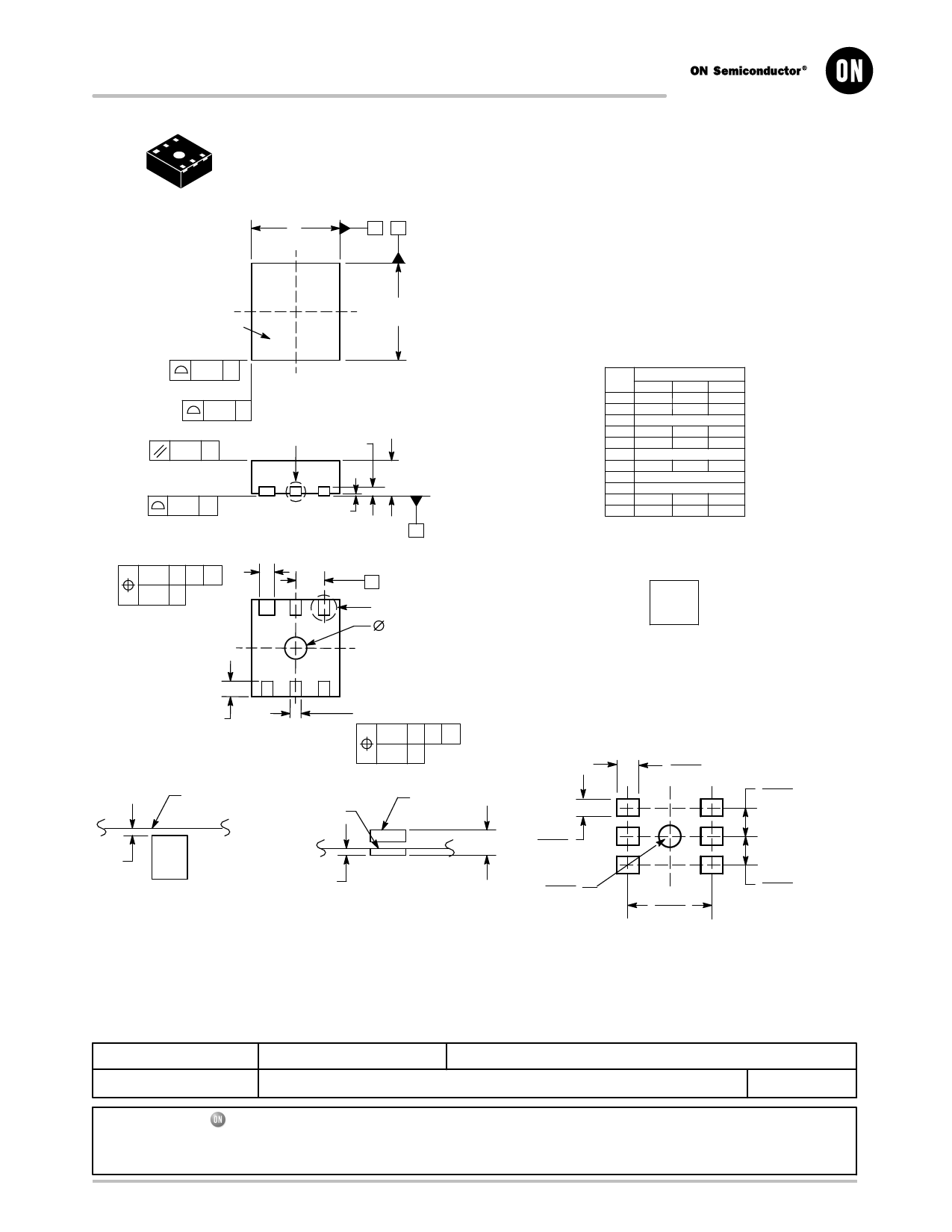
MECHANICAL CASE OUTLINE
PACKAGE DIMENSIONS
DFN6 2x2.2 mm
CASE 488−03
ISSUE G
DATE 06 FEB 2006
SCALE 4:1
D
AB
2X
PIN ONE
ÍÍÍ REFERENCE
ÍÍÍÍÍÍ 0.10 C
E
TOP VIEW
2X
0.10 C
0.10 C
6X
0.08 C
DETAIL B
A3
A
A1
SIDE VIEW
C
SEATING
PLANE
0.10 C A B b1
0.05 C NOTE 3
1
e
3
DETAIL A
D2
NOTES:
1. DIMENSIONING AND TOLERANCING PER
ASME Y14.5M, 1994.
2. CONTROLLING DIMENSION: MILLIMETERS.
3. DIMENSION b APPLIES TO PLATED
TERMINAL AND IS MEASURED BETWEEN
0.25 AND 0.30mm FROM TERMINAL.
4. COPLANARITY APPLIES TO THE EXPOSED
PAD AS WELL AS THE TERMINALS.
5. TERMINAL b MAY HAVE MOLD COMPOUND
MATERIAL ALONG SIDE EDGE.
6. DETAILS A AND B SHOW OPTIONAL VIEWS
FOR END OF TERMINAL LEAD AT EDGE OF
PACKAGE AND SIDE EDGE OF PACKAGE.
MILLIMETERS
DIM MIN NOM MAX
A 0.80 0.90 1.00
A1 0.00 0.03 0.05
A3
0.20 REF
b 0.20 0.25 0.30
b1 0.30 0.35 0.40
D
2.00 BSC
D2 0.40 0.50 0.60
E
2.20 BSC
e
0.65 BSC
L 0.30 0.35 0.40
L1 0.00 0.05 0.10
GENERIC
MARKING DIAGRAM*
xxM
xx = Specific Device Code
M = Date Code
6
6X L
4
b 5X
0.10 C A B
*This information is generic. Please refer
to device data sheet for actual part
marking.
SOLDERING FOOTPRINT*
BOTTOM VIEW
0.05 C NOTE 3
0.50
0.020
0.65
L1
EDGE OF PACKAGE
MOLD CMPD
EXPOSED Cu
ÉÉÉÉ A3
0.40
0.016
0.025
DETAIL A
Bottom View
(Optional)
A1
DETAIL B
Side View
(Optional)
0.50
0.020
1.9
0.075
0.65
0.025
SCALE 10:1
*For additional information on our Pb−Free strategy and soldering
details, please download the ON Semiconductor Soldering and
Mounting Techniques Reference Manual, SOLDERRM/D.
DOCUMENT NUMBER:
DESCRIPTION:
98AON04199D
Electronic versions are uncontrolled except when accessed directly from the Document Repository.
Printed versions are uncontrolled except when stamped “CONTROLLED COPY” in red.
DFN6 2 X 2.2 X 0.9 X 0.65P
PAGE 1 OF 1
ON Semiconductor and
are trademarks of Semiconductor Components Industries, LLC dba ON Semiconductor or its subsidiaries in the United States and/or other countries.
ON Semiconductor reserves the right to make changes without further notice to any products herein. ON Semiconductor makes no warranty, representation or guarantee regarding
the suitability of its products for any particular purpose, nor does ON Semiconductor assume any liability arising out of the application or use of any product or circuit, and specifically
disclaims any and all liability, including without limitation special, consequential or incidental damages. ON Semiconductor does not convey any license under its patent rights nor the
rights of others.
© Semiconductor Components Industries, LLC, 2019
www.onsemi.com
Share Link: