NX3P1107 데이터 시트보기 (PDF) - NXP Semiconductors.
부품명
상세내역
제조사
NX3P1107 Datasheet PDF : 16 Pages
| |||
NXP Semiconductors
NX3P1107
Logic controlled high-side power switch
4. Ordering information
Table 1. Ordering information
Type number Package
Temperature range
NX3P1107UK 40 C to +85 C
Name Description
Version
WLCSP4 wafer level chip-size package; 4 bumps; 0.96 NX3P1107/NX3P1108
0.96 0.55 mm. (Backside coating included)
5. Marking
Table 2. Marking codes
Type number
NX3P1107UK
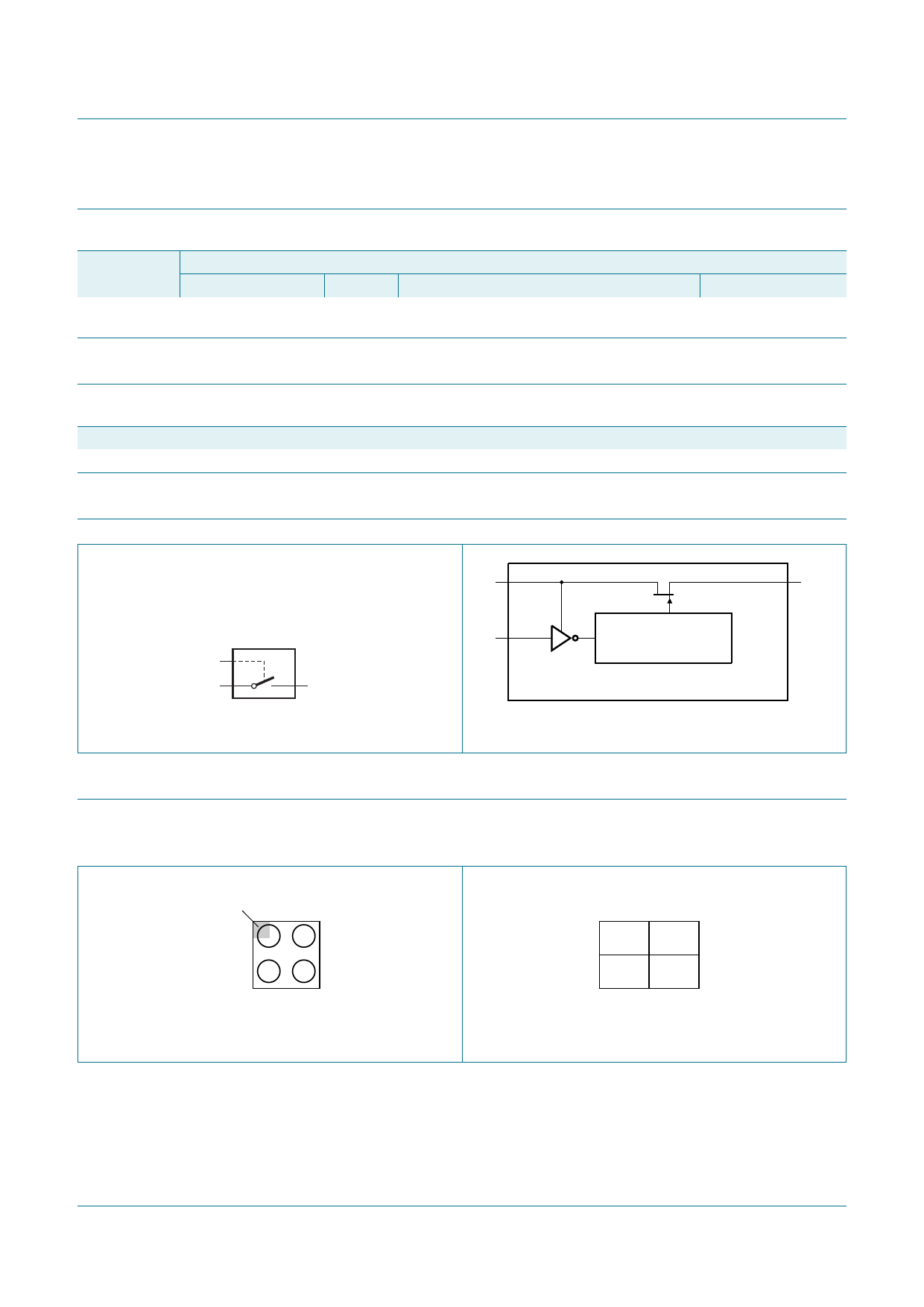
6. Functional diagram
Marking code
x7
EN
VIN
VOUT
001aao342
Fig 1. Logic symbol
7. Pinning information
7.1 Pinning
EXPS $ 1;3
LQGH[ DUHD
$
%
DDD
7UDQVSDUHQW WRS YLHZ
Fig 3. Pin configuration for WLCSP4
9,1
9287
(1
/(9(/ 6+,)7 $1'
6/(: 5$7( &21752/
DDD
Fig 2. Logic diagram (simplified schematic)
$ 9287 9,1
% *1'
(1
DDD
7UDQVSDUHQW WRS YLHZ
Fig 4. Ball mapping for WLCSP4
NX3P1107
Product data sheet
All information provided in this document is subject to legal disclaimers.
Rev. 1 — 9 January 2013
© NXP B.V. 2013. All rights reserved.
2 of 16
Share Link: 