NCP4586 데이터 시트보기 (PDF) - ON Semiconductor
부품명
상세내역
제조사
NCP4586 Datasheet PDF : 18 Pages
| |||
NCP4586
APPLICATION INFORMATION
A typical application circuit for NCP4586 series is shown
in Figure 42.
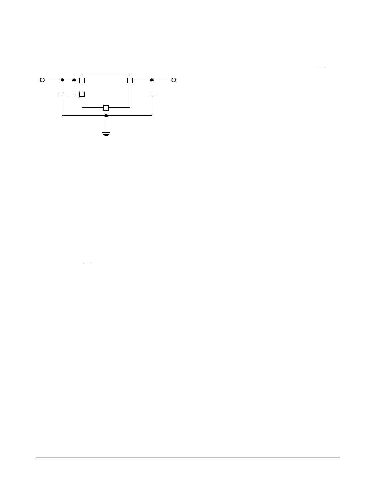
VIN
C1
470n
NCP 4586 x
VIN VOUT
CE
GND
VOUT
C2
470n
version of IC. Active high or low versions are available;
please see the ordering information table. The Enable pin
has an internal pull down current source for versions H and
D. If the enable function is not needed connect the CE pin to
ground for version L or connect the CE pin to VIN for
versions H and D.
Output Discharger
The D version includes a transistor between VOUT and
GND that is used for faster discharging of the output
capacitor. This function is activated when the IC goes into
disable mode.
Figure 42. Typical Application Schematic
Input Decoupling Capacitor (C1)
A 470 nF ceramic input decoupling capacitor should be
connected as close as possible to the input and ground pin of
the NCP4586. Higher values and lower ESR improves line
transient response.
Output Decoupling Capacitor (C2)
A 470 nF or larger ceramic output decoupling capacitor is
sufficient to achieve stable operation of the IC. If a tantalum
capacitor is used, and its ESR is high, loop oscillation may
result. The capacitors should be connected as close as
possible to the output and ground pins. Larger values and
lower ESR improves dynamic parameters.
Enable Operation
The Enable pin CE or CE may be used for turning the
regulator on and off. Control polarity is dependent on
Thermal
As power across the IC increases, it might become
necessary to provide some thermal relief. The maximum
power dissipation supported by the device is dependent
upon board design and layout. Mounting pad configuration
on the PCB, the board material, and also the ambient
temperature affect the rate of temperature rise for the part.
That is to say, when the device has good thermal
conductivity through the PCB, the junction temperature will
be relatively low with high power dissipation applications.
PCB Layout
Make VIN and GND line sufficient. If their impedance is
high, noise pickup or unstable operation may result. Connect
capacitors C1 and C2 as close as possible to the IC, and make
wiring as short as possible.
http://onsemi.com
14
Share Link: 