NT5CB128M8DN-FK 데이터 시트보기 (PDF) - Nanya Technology
부품명
상세내역
제조사
NT5CB128M8DN-FK Datasheet PDF : 138 Pages
| |||
NT5CB128M8DN/NT5CB64M16DP
NT5CC128M8DN/NT5CC64M16DP
1Gb DDR3 D-die SDRAM
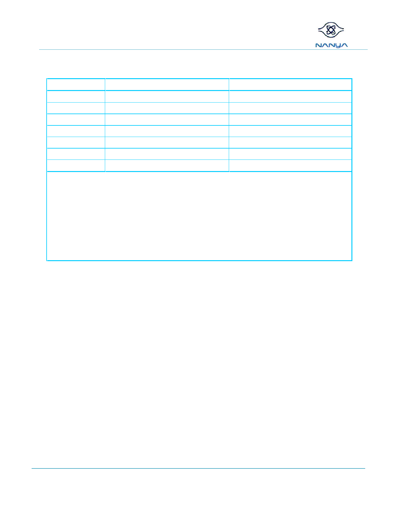
Table 3: DDR3/L SDRAM Addressing
Configuration
NT5CB128M8DN/NT5CC128M8DN
NT5CB64M16DP/NT5CC64M16DP
# of Bank
8
8
Bank Address
BA0 – BA2
BA0 – BA2
Auto precharge
A10 / AP
A10 / AP
BL switch on the fly
A12 /
A12 /
Row Address
A0 – A13
A0 – A12
Column Address
A0 – A9
A0 – A9
Page size
1KB
2KB
Note:
Page size is the number of data delivered from the array to the internal sense amplifiers when an ACTIVE command is
registered. Page size is per bank, calculated as follows:
Page size = 2 COLBITS * ORG / 8
COLBITS = the number of column address bits
ORG = the number of I/O (DQ) bits
REV 1.2
May. 2011
CONSUMER DRAM
© NANYA TECHNOLOGY CORP.
All rights reserved
NANYA TECHNOLOGY CORP. reserves the right to change Products and Specifications without notice.
Share Link: 