AS3932 데이터 시트보기 (PDF) - austriamicrosystems AG
부품명
상세내역
제조사
AS3932 Datasheet PDF : 33 Pages
| |||
AS3932
Data Sheet - Detailed Description
Table 12. List of Direct Commands
COMMAND_MODE
trim_osc
clear_false
preset_default
B13
B12
B11
B10
B9
B8
0
0
0
0
1
0
0
0
0
0
1
1
0
0
0
1
0
0
All direct commands are explained below:
- clear_wake: clears the wake state of the chip. In case the chip has woken up (WAKE pin is high) the chip is set back to listening mode
- reset_RSSI: resets the RSSI measurement.
- trim_osc: starts the trimming procedure of the internal RC oscillator (see Figure 22)
- clear_false: resets the false wakeup register (R13=00)
- preset_default: sets all register in the default mode, as shown in Figure 7
8.3.3.2 Writing of Data to Addressable Registers (WRITE Mode)
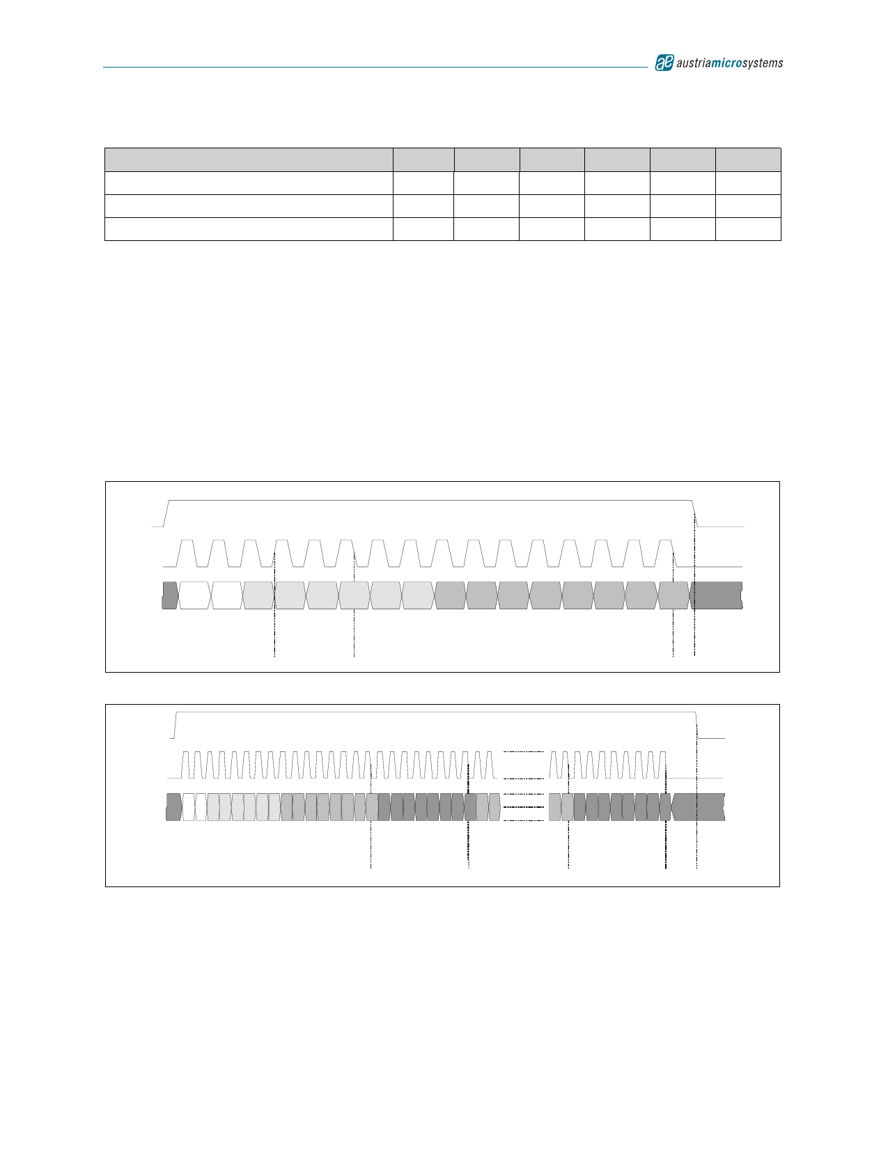
The SDI is sampled at the falling edge of CLK (as shown in the following diagrams).
A CS toggling high-low-high indicates the end of the WRITE command after register has been written. The following example shows a write
command.
Figure 13. Writing of a Single Byte (falling edge sampling)
CS
S CLK
SDI
X
0
0
A5
A4
A3
A2
A1 A0
D7
D6
D5 D 4
D3
D2 D1
D0
X
Two leading
Zeros indicate
WRITE Mode
SCLK raising
edge Data is
transfered from
µC
SCLK
falling edge
Data is
sampled
Data is moved
to Address
A5- A 0
CS falling
edge signals
end of
WRITE Mode
Figure 14. Writing of Register Data with Auto-incrementing Address
CS
S CLK
SDI
X
0
0
A
5
AA
43
AA
21
AD
07
DDDD
6543
D
2
DD
10
DD
76
DDD
543
D DDD
21 07
D
6
DD DDD D DD DD
X
107 65 43 2 10
Two leading
Zeros indicate
WRITE Mode
Data is moved
to Address
<A 5- A 0 >
Dat a is mov ed
to Addres s
<A5-A0> +1
Data is moved
to Addres s
<A5-A0 > + (n- 1)
Data is moved
to Address
<A5-A0 > + n
CS falling
edge signals
end of
WRITE Mode
8.3.3.3 Reading of Data from Addressable Registers (READ Mode)
Once the address has been sent through SDI, the data can be fed through the SDO pin out to the microcontroller.
A CS LOW toggling high-low-high has to be performed after finishing the read mode session, in order to indicate the end of the READ command
and prepare the Interface to the next command control Byte.
To transfer bytes from consecutive addresses, SDI master has to keep the CS signal high and the SCLK clock has to be active as long as data
need to be read.
www.austriamicrosystems.com/AS3932
Revision 1.2
17 - 33
Share Link: 