BFT92W 데이터 시트보기 (PDF) - Philips Electronics
부품명
상세내역
제조사
BFT92W Datasheet PDF : 12 Pages
| |||
Philips Semiconductors
PNP 4 GHz wideband transistor
Product specification
BFT92W
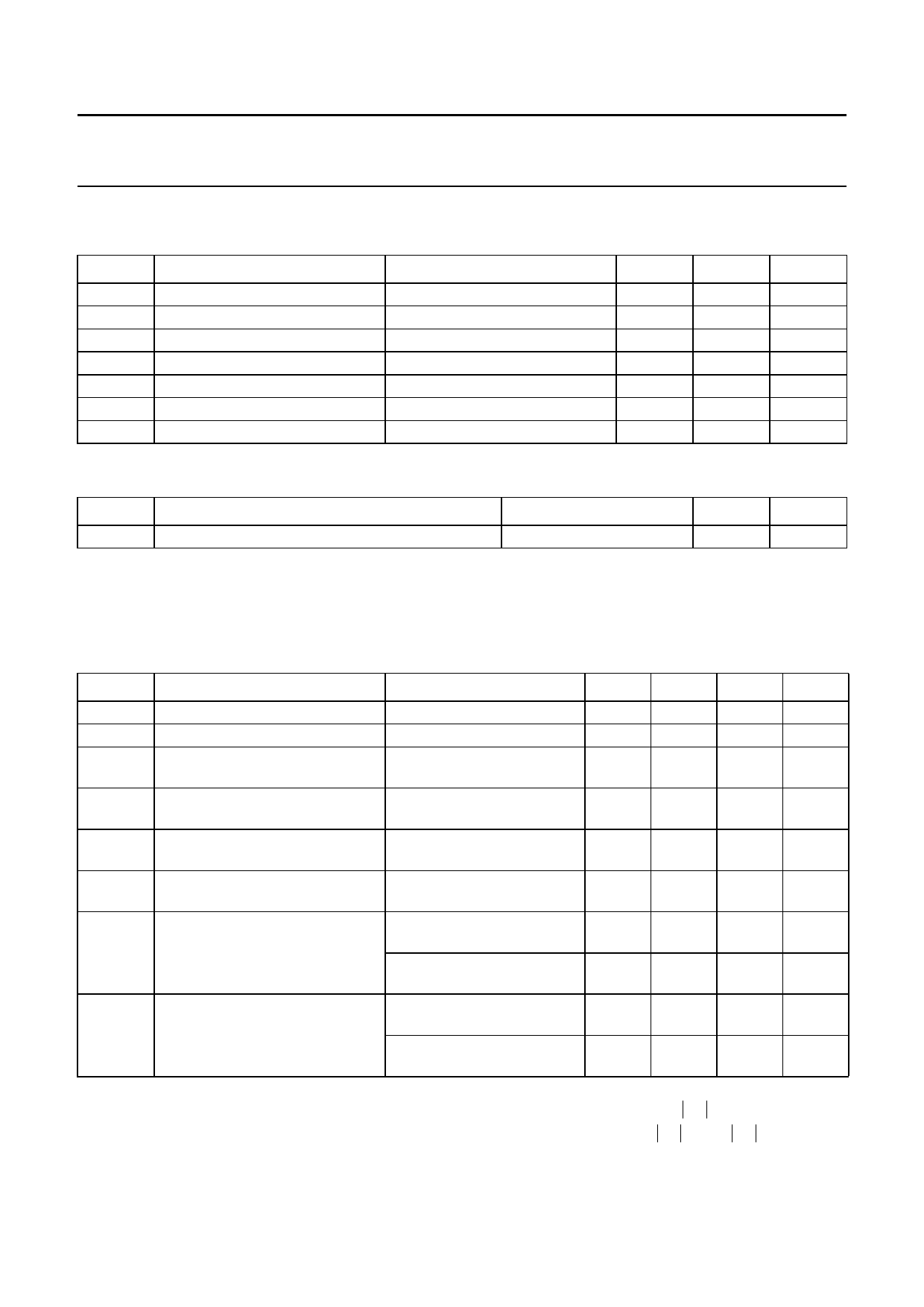
LIMITING VALUES
In accordance with the Absolute Maximum Rating System (IEC 134).
SYMBOL
PARAMETER
CONDITIONS
VCBO
VCEO
VEBO
IC
Ptot
Tstg
Tj
collector-base voltage
collector-emitter voltage
emitter-base voltage
collector current (DC)
total power dissipation
storage temperature
junction temperature
open emitter
open base
open collector
up to Ts = 93 °C; note 1
MIN.
−
−
−
−
−
−65
−
MAX.
−20
−15
−2
−25
300
+150
150
UNIT
V
V
V
mA
mW
°C
°C
THERMAL CHARACTERISTICS
SYMBOL
PARAMETER
CONDITIONS
Rth j-s
thermal resistance from junction to soldering point up to Ts = 93 °C; note 1
Note to the “Limiting values” and “Thermal characteristics”
1. Ts is the temperature at the soldering point of the collector pin.
VALUE
190
UNIT
K/W
CHARACTERISTICS
Tj = 25 °C (unless otherwise specified).
SYMBOL
PARAMETER
ICBO
collector cut-off current
hFE
DC current gain
fT
transition frequency
Cc
collector capacitance
Ce
emitter capacitance
Cre
feedback capacitance
GUM
maximum unilateral power gain;
note 1
F
noise figure
CONDITIONS
IE = 0; VCB = −10 V
IC = −15 mA; VCE = −10 V
IC = −15 mA; VCE = −10 V;
f = 500 MHz; Tamb = 25 °C
IE = ie = 0; VCB = −10 V;
f = 1 MHz
IC = ic = 0; VEB = −0.5 V;
f = 1 MHz
IC = 0; VCB = −10 V;
f = 1 MHz
IC = −15 mA; VCE = −10 V;
f = 500 MHz; Tamb = 25 °C
IC = −15 mA; VCE = −10 V;
f = 1 GHz; Tamb = 25 °C
Γs = Γopt; IC = −5 mA;
VCE = −10 V; f = 500 MHz
Γs = Γopt; IC = −5 mA;
VCE = −10 V; f = 1 GHz
MIN.
−
20
−
TYP.
−
50
4
MAX.
−50
−
−
UNIT
nA
GHz
−
0.65
−
pF
−
0.75
−
pF
−
0.5
−
pF
−
17
−
dB
−
11
−
dB
−
2.5
−
dB
−
3
−
dB
Note
1. GUM is the maximum unilateral power gain, assuming s12 is zero. GUM
=
10
log --(--1-----–------s---1---1----2s---)-2--1-(---1-2----–------s---2--2-----2---)-
dB.
May 1994
3
Share Link: 