LC75810E 데이터 시트보기 (PDF) - ON Semiconductor
부품명
상세내역
제조사
LC75810E Datasheet PDF : 54 Pages
| |||
LC75810E/T
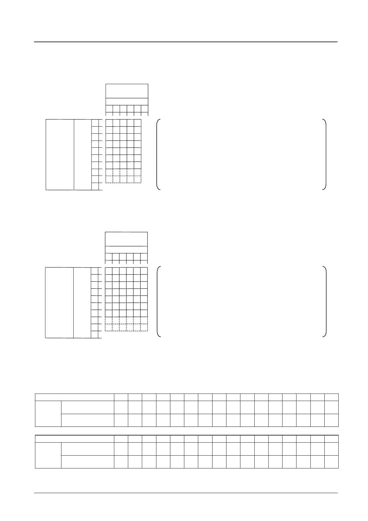
∗19 The figure below lists the correspondence between the data HA0 to HA2 which is dot address in the horizontal
direction and the dot matrix character pattern, and the correspondence between the data VA0 to VA3 which is dot
address in the vertical direction and the dot matrix character pattern.
• 5-dot font width: 5 × 7, 5 × 8, or 5 × 9 dots
Dot address in the
horizontal direction
HA0 to HA2 (HEX)
012345
0
1
Dot address in VA0 to 2
the vertical VA3 3
direction
(HEX) 4
5
6
7
8
9
• The area at HA0 to 2 = 5H is allocated to the space at the right of
the dot matrix character pattern.
• The area at VA0 to 3 = 7H, for 5 × 7 dot characters, is allocated to
the space at the bottom of the dot matrix character pattern.
• The area at VA0 to 3 = 8H is illegal for 5 × 7 dot characters. For 5
× 8 dot characters, it is allocated to the space at the bottom of the
dot matrix character pattern.
• The area at VA0 to 3 = 9H is illegal for 5 × 7 or 5 × 8 dot
characters. For 5 × 9 dot characters, it is allocated to the space at
the bottom of the dot matrix character pattern.
• 6-dot font width: 6 × 7, 6 × 8, or 6 × 9 dots
0
1
2
Dot address in VA0 to 3
the vertical
VA3 4
direction
(HEX) 5
6
7
8
9
Dot address in the
horizontal direction
HA0 to HA2 (HEX)
012345
• The area at HA0 to 2 = 5H is allocated to the space at the right of
the dot matrix character pattern.
• The area at VA0 to 3 = 7H, for 6 × 7 dot characters, is allocated to
the space at the bottom of the dot matrix character pattern.
• The area at VA0 to 3 = 8H is illegal for 6 × 7 dot characters. For 6
× 8 dot characters, it is allocated to the space at the bottom of the
dot matrix character pattern.
• The area at VA0 to 3 = 9H is illegal for 6 × 7 or 6 × 8 dot
characters. For 6 × 9 dot characters, it is allocated to the space at
the bottom of the dot matrix character pattern.
∗20: Example of the “set AC and SC addresses” instruction execution
Assume that a 32 digits × 2 lines display structure (OZ1 = 1, OZ2 = 0) has been set up with the “set display technique”
instruction, and that the following data has been written to DCRAM with the “DCRAM data write” instruction.
Display digit
1
2
3
4
5
6
7
8
9 10 11 12 13 14 15 16
DCRAM
data
First line (DCRAM
A
B
C
D
E
F
G
H
I
J
K
L
M
N
O
P
address (hexadecimal)) (00) (01) (02) (03) (04) (05) (06) (07) (08) (09) (0A) (0B) (0C) (0D) (0E) (0F)
Second line (DCRAM
0
1
2
3
4
5
6
7
8
9
a
b
c
d
e
f
address (hexadecimal)) (20) (21) (22) (23) (24) (25) (26) (27) (28) (29) (2A) (2B) (2C) (2D) (2E) (2F)
Display digit
17 18 19 20 21 22 23 24 25 26 27 28 29 30 31 32
DCRAM
data
First line (DCRAM
QRS
T
U VWX
Y
Z
<
>
z
y
x
w
address (hexadecimal)) (10) (11) (12) (13) (14) (15) (16) (17) (18) (19) (1A) (1B) (1C) (1D) (1E) (1F)
Second line (DCRAM
g
h
i
j
k
l
mn
o
p
q
r
s
t
u
v
address (hexadecimal)) (30) (31) (32) (33) (34) (35) (36) (37) (38) (39) (3A) (3B) (3C) (3D) (3E) (3F)
No.7141-18/54
Share Link: 