Q62702-G0071 데이터 시트보기 (PDF) - Siemens AG
부품명
상세내역
제조사
Q62702-G0071 Datasheet PDF : 8 Pages
| |||
CGY 121 B
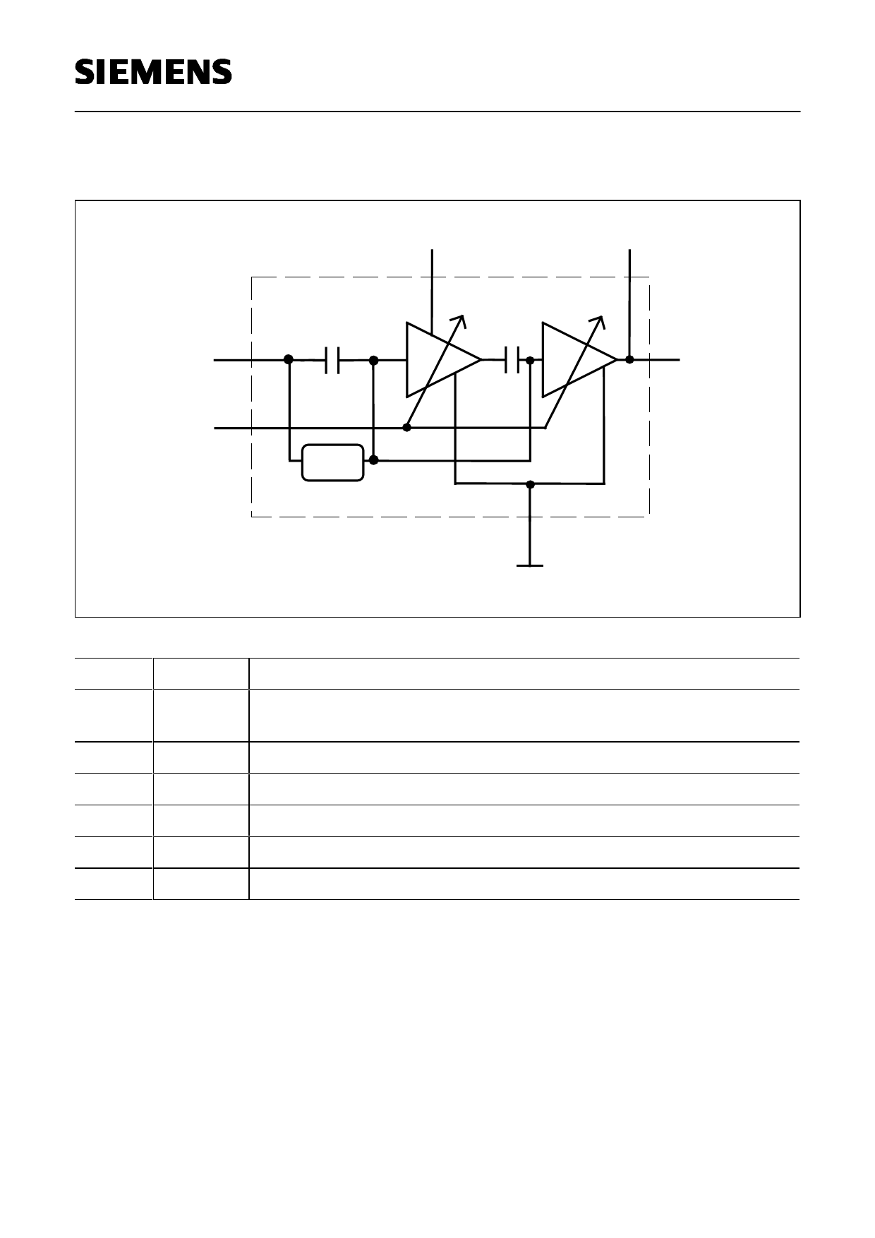
Functional block diagram:
Pin / -VG(4)
Vcon (6)
Control
Circuit
VD1 (3)
VD2 (1)
Pout (1)
GND (2, 5)
Pin #
1
2
3
4
5
6
Configuration
VD2 / Drain voltage 2nd stage / RF-0utput
Pout
RF-Gnd
VD1 Drain voltage 1st stage
VG / Pin Negative voltage at current control circuit (-4V) / RF-Input
RF-Gnd
Vcontrol Positive voltage for gain control (0V....3V)
Siemens Aktiengesellschaft
2
Semiconductor Group
2
04.08.98
HL HF PE GaAs/HB
1998-11-01
Share Link: 