MTW7N80E 데이터 시트보기 (PDF) - ON Semiconductor
부품명
상세내역
제조사
MTW7N80E Datasheet PDF : 8 Pages
| |||
MTW7N80E
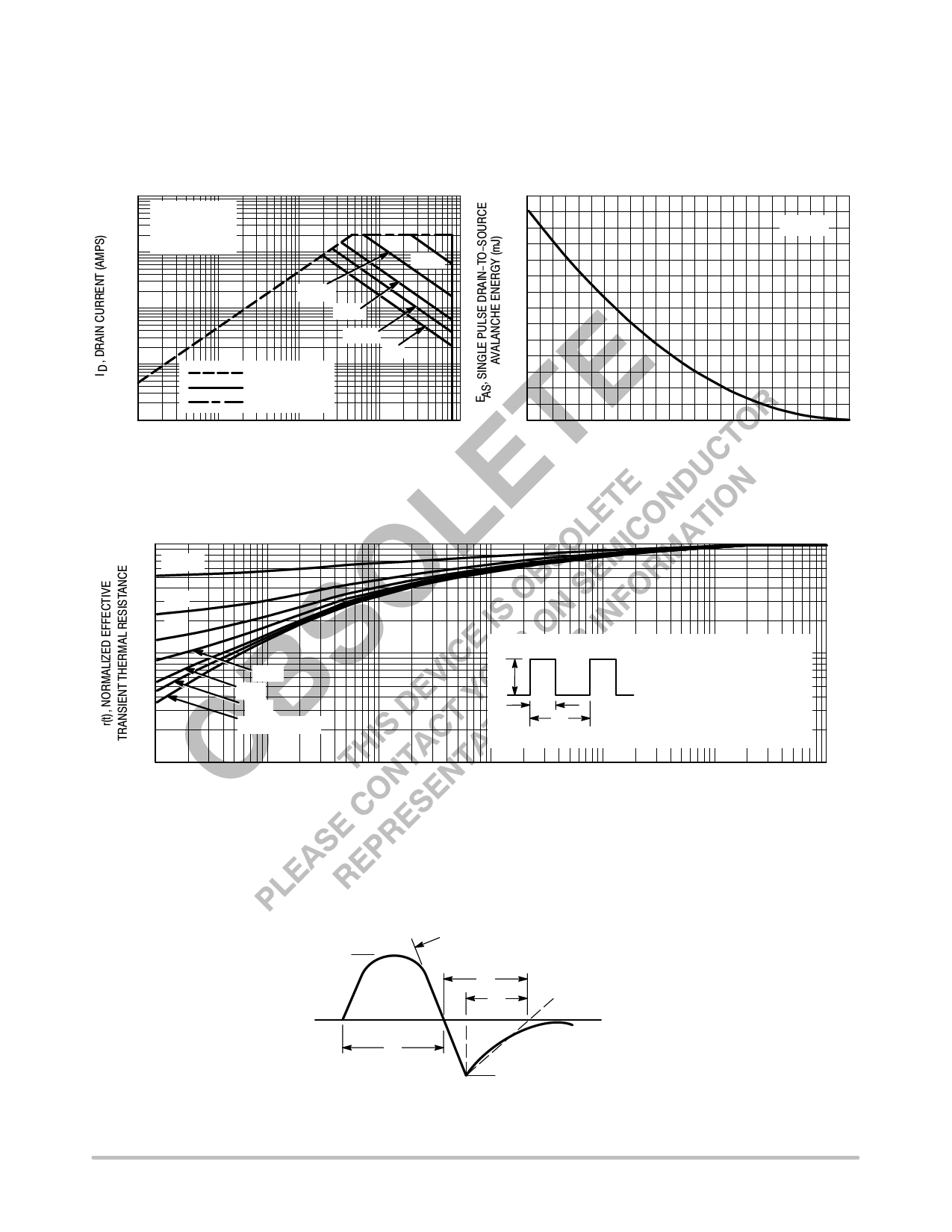
as shown in the accompanying graph (Figure 12). Maximum
energy at currents below rated continuous ID can safely be
assumed to equal the values indicated.
SAFE OPERATING AREA
100
VGS = 20 V
SINGLE PULSE
10 TC = 25°C
10 µs
100 µs
1.0
1 ms
10 ms
dc
0.1
RDS(on) LIMIT
THERMAL LIMIT
PACKAGE LIMIT
0.01
0.1
1.0
10
100
1000
VDS, DRAIN−TO−SOURCE VOLTAGE (VOLTS)
Figure 11. Maximum Rated Forward Biased
Safe Operating Area
700
600
ID = 7 A
500
400
300
200
100
0
25
50
75
100
125
150
TJ, STARTING JUNCTION TEMPERATURE (°C)
Figure 12. Maximum Avalanche Energy versus
Starting Junction Temperature
1.0
D = 0.5
0.2
0.1
0.1
0.01
1.0E−05
0.05
0.02
0.01
SINGLE PULSE
1.0E−04
P(pk)
t1
t2
DUTY CYCLE, D = t1/t2
RθJC(t) = r(t) RθJC
D CURVES APPLY FOR POWER
PULSE TRAIN SHOWN
READ TIME AT t1
TJ(pk) − TC = P(pk) RθJC(t)
1.0E−03
1.0E−02
t, TIME (s)
1.0E−01
Figure 13. Thermal Response
1.0E+00
1.0E+01
IS
tp
di/dt
trr
ta
tb
0.25 IS
IS
TIME
Figure 14. Diode Reverse Recovery Waveform
http://onsemi.com
6
Share Link: 