NCP500(2004) 데이터 시트보기 (PDF) - ON Semiconductor
부품명
상세내역
제조사
NCP500 Datasheet PDF : 20 Pages
| |||
NCP500
Input
Enable
1
1.0 mF
2
3
1
1.0 mF
2
3
R
C
Output
5
1.0 mF
4
Output
5
1.0 mF
4
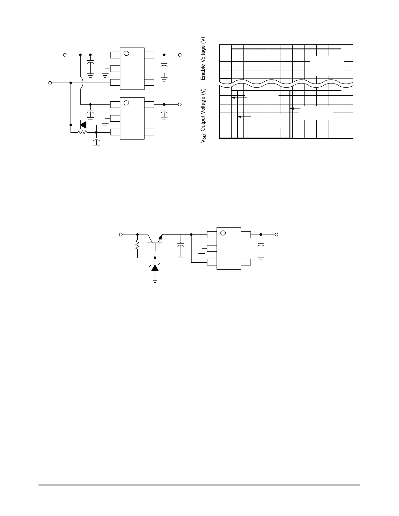
Figure 32. Delayed Turn−on
If a delayed turn−on is needed during power up of several volt-
ages then the above schematic can be used. Resistor R, and
capacitor C, will delay the turn−on of the bottom regulator. A
few values were chosen and the resulting delay can be seen in
Figure 33.
4
3
2
TA = 25°C
Vin = 3.4 V
1
Vout = 2.8 V
0
3
2.5
No Delay
2
1.5
R = 1.0 MW
R = 1.0 MW
C = 1.0 mF
1
C = 0.1 mF
0.5
0
0 10 20 30 40 50 60 70 80 90 100 110
Time (ms)
Figure 33. Delayed Turn−on
The graph shows the delay between the enable signal and
output turn−on for various resistor and capacitor values.
Input
R
Q1
1.0 mF
5.6 V
Output
1
5
1.0 mF
2
3
4
Figure 34. Input Voltages Greater than 6.0 V
A regulated output can be achieved with input voltages that ex-
ceed the 6.0 V maximum rating of the NCP500 series with the
addition of a simple pre−regulator circuit. Care must be taken
to prevent Q1 from overheating when the regulated output
(Vout) is shorted to Gnd.
http://onsemi.com
16
Share Link: 