M24C16-X 데이터 시트보기 (PDF) - STMicroelectronics
부품명
상세내역
제조사
M24C16-X Datasheet PDF : 38 Pages
| |||
M24C16, M24C08, M24C04, M24C02, M24C01
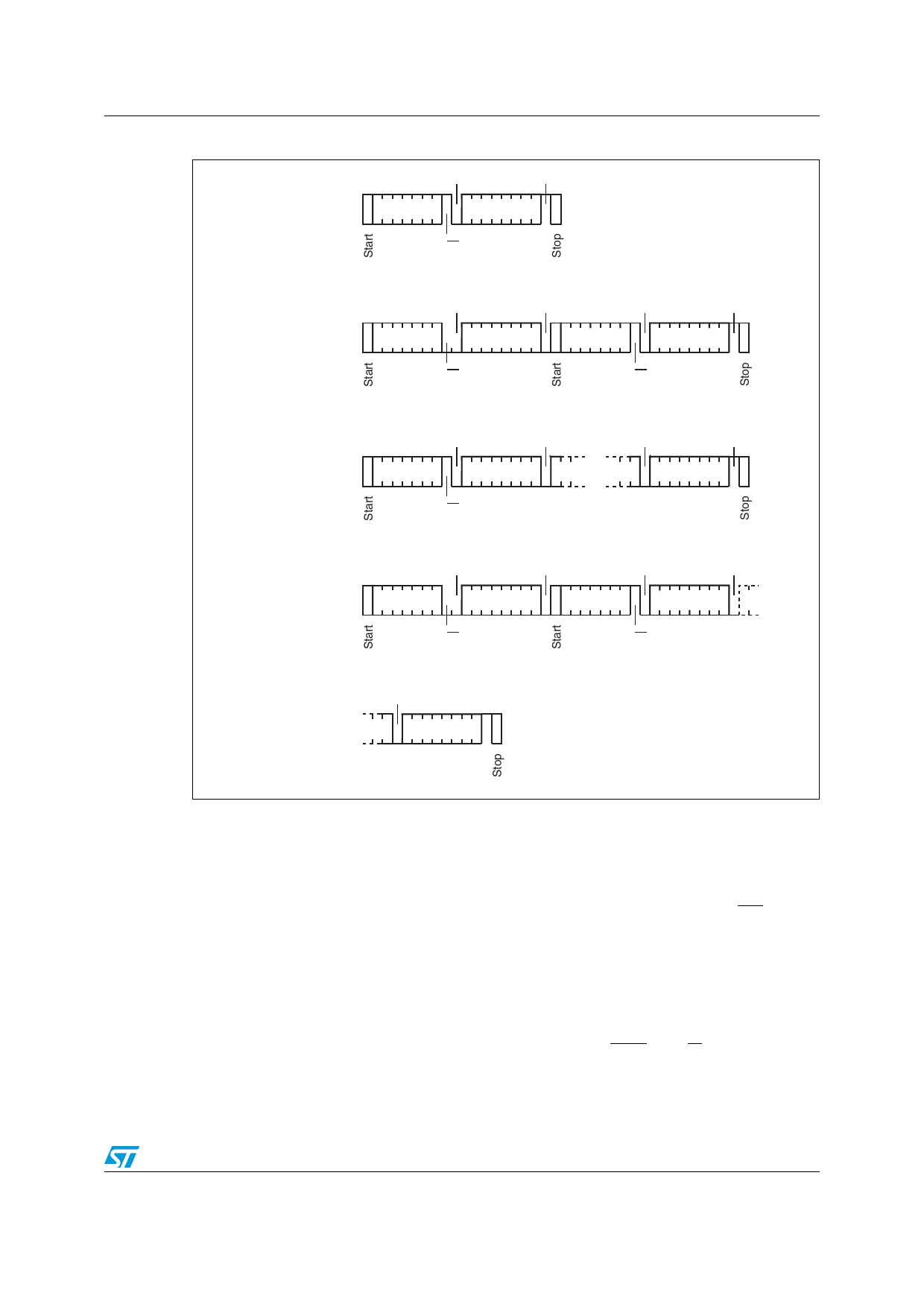
Figure 10. Read mode sequences
Current
Address
Read
ACK
NO ACK
Dev select
Data out
R/W
Device operation
Random
Address
Read
ACK
ACK
ACK
NO ACK
Dev select * Byte address Dev select *
Data out
R/W
R/W
Sequentila
Current
Read
ACK
ACK
Dev select
Data out 1
R/W
ACK
NO ACK
Data out N
Sequential
Random
Read
ACK
ACK
ACK
ACK
Dev select * Byte address Dev select *
Data out 1
R/W
R/W
ACK
NO ACK
Data out N
3.7
3.7.1
AI01942b
1. The seven most significant bits of the device select code of a Random Read (in the 1st and 3rd bytes) must
be identical.
Read operations
Read operations are performed independently of the state of the Write Control (WC) signal.
The device has an internal address counter which is incremented each time a byte is read.
Random Address Read
A dummy Write is first performed to load the address into this address counter (as shown in
Figure 10) but without sending a Stop condition. Then, the bus master sends another Start
condition, and repeats the device select code, with the Read/Write bit (RW) set to 1. The
device acknowledges this, and outputs the contents of the addressed byte. The bus master
must not acknowledge the byte, and terminates the transfer with a Stop condition.
Doc ID 5067 Rev 17
17/38
Share Link: 