ADR292ER 데이터 시트보기 (PDF) - Analog Devices
부품명
상세내역
제조사
ADR292ER Datasheet PDF : 15 Pages
| |||

ADR290/ADR291/ADR292
THEORY OF OPERATION
The ADR29x series of references uses a new reference generation
technique known as XFET (eXtra implanted junction FET). This
technique yields a reference with low noise, low supply current
and very low thermal hysteresis.
The core of the XFET reference consists of two junction field-
effect transistors, one of which has an extra channel implant to
raise its pinch-off voltage. By running the two JFETS at the
same drain current, the difference in pinch-off voltage can be
amplified and used to form a highly stable voltage reference.
The intrinsic reference voltage is around 0.5 V with a negative
temperature coefficient of about –120 ppm/K. This slope is es-
sentially locked to the dielectric constant of silicon and can be
closely compensated by adding a correction term generated in
the same fashion as the proportional-to-temperature (PTAT)
term used to compensate bandgap references. The big advan-
tage over a bandgap reference is that the intrinsic temperature
coefficient is some thirty times lower (therefore less correction is
needed) and this results in much lower noise since most of the
noise of a bandgap reference comes from the temperature com-
pensation circuitry.
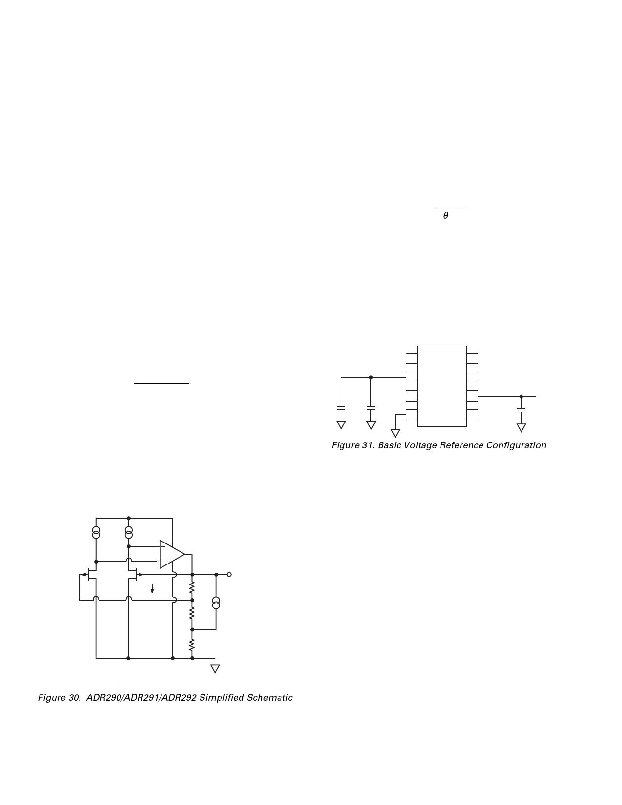
The simplified schematic below shows the basic topology of the
ADR29x series. The temperature correction term is provided by
a current source with value designed to be proportional to abso-
lute temperature. The general equation is:
( )( ) VOUT
=
∆VP
R1
+
R2
R1
+
R3
+
I PTAT
R3
where ∆VP is the difference in pinch-off voltage between the two
FETs, and IPTAT is the positive temperature coefficient correc-
tion current. The various versions of the ADR29x family are
created by on-chip adjustment of R1 and R3 to achieve 2.048 V,
2.500 V or 4.096 V at the reference output.
The process used for the XFET reference also features vertical
NPN and PNP transistors, the latter of which are used as output
devices to provide a very low drop-out voltage.
VIN
I1 I1
*
∆VP
VOUT
R1
IPTAT
R2
R3
*EXTRA CHANNEL IMPLANT
VOUT ؍R1؉R2؉R3 ؋ ∆VP؉ IPTAT ؋R3
R1
GND
Figure 30. ADR290/ADR291/ADR292 Simplified Schematic
Device Power Dissipation Considerations
The ADR29x family of references is guaranteed to deliver load
currents to 5 mA with an input voltage that ranges from 2.7 V
to 15 V (minimum supply voltage depends on output voltage
option). When these devices are used in applications with large
input voltages, care should be exercised to avoid exceeding the
published specifications for maximum power dissipation or
junction temperature that could result in premature device fail-
ure. The following formula should be used to calculate a device’s
maximum junction temperature or dissipation:
PD
=
TJ − TA
θ JA
In this equation, TJ and TA are the junction and ambient tem-
peratures, respectively, PD is the device power dissipation, and
θJA is the device package thermal resistance.
Basic Voltage Reference Connections
References, in general, require a bypass capacitor connected
from the VOUT pin to the GND pin. The circuit in Figure 31
illustrates the basic configuration for the ADR29x family of ref-
erences. Note that the decoupling capacitors are not required
for circuit stability.
+
10F
NC 1
2
NC 3
0.1F
4
ADR29x
8 NC
7 NC
OUTPUT
6
5 NC
0.1F
Figure 31. Basic Voltage Reference Configuration
Noise Performance
The noise generated by the ADR29x family of references is typi-
cally less than 12 µV p-p over the 0.1 Hz to 10 Hz band. Figure
21 shows the 0.1 Hz to 10 Hz noise of the ADR290 which is
only 6 µV p-p. The noise measurement is made with a bandpass
filter made of a 2-pole high-pass filter with a corner frequency at
0.1 Hz and a 2-pole low-pass filter with a corner frequency at
10 Hz.
Turn-On Time
Upon application of power (cold start), the time required for the
output voltage to reach its final value within a specified error
band is defined as the turn-on settling time. Two components
normally associated with this are the time for the active circuits
to settle, and the time for the thermal gradients on the chip to
stabilize. Figure 28 shows the turn-on settling time for the
ADR291.
APPLICATIONS SECTION
A Negative Precision Reference without Precision Resistors
In many current-output CMOS DAC applications, where the
output signal voltage must be of the same polarity as the refer-
ence voltage, it is often required to reconfigure a current-switch-
ing DAC into a voltage-switching DAC through the use of a
1.25 V reference, an op amp and a pair of resistors. Using a cur-
rent-switching DAC directly requires the need for an additional
operational amplifier at the output to reinvert the signal. A
negative voltage reference is then desirable from the point that
–12–
REV. A