ADSP-BF539F(RevA) 데이터 시트보기 (PDF) - Analog Devices
부품명
상세내역
제조사
ADSP-BF539F Datasheet PDF : 60 Pages
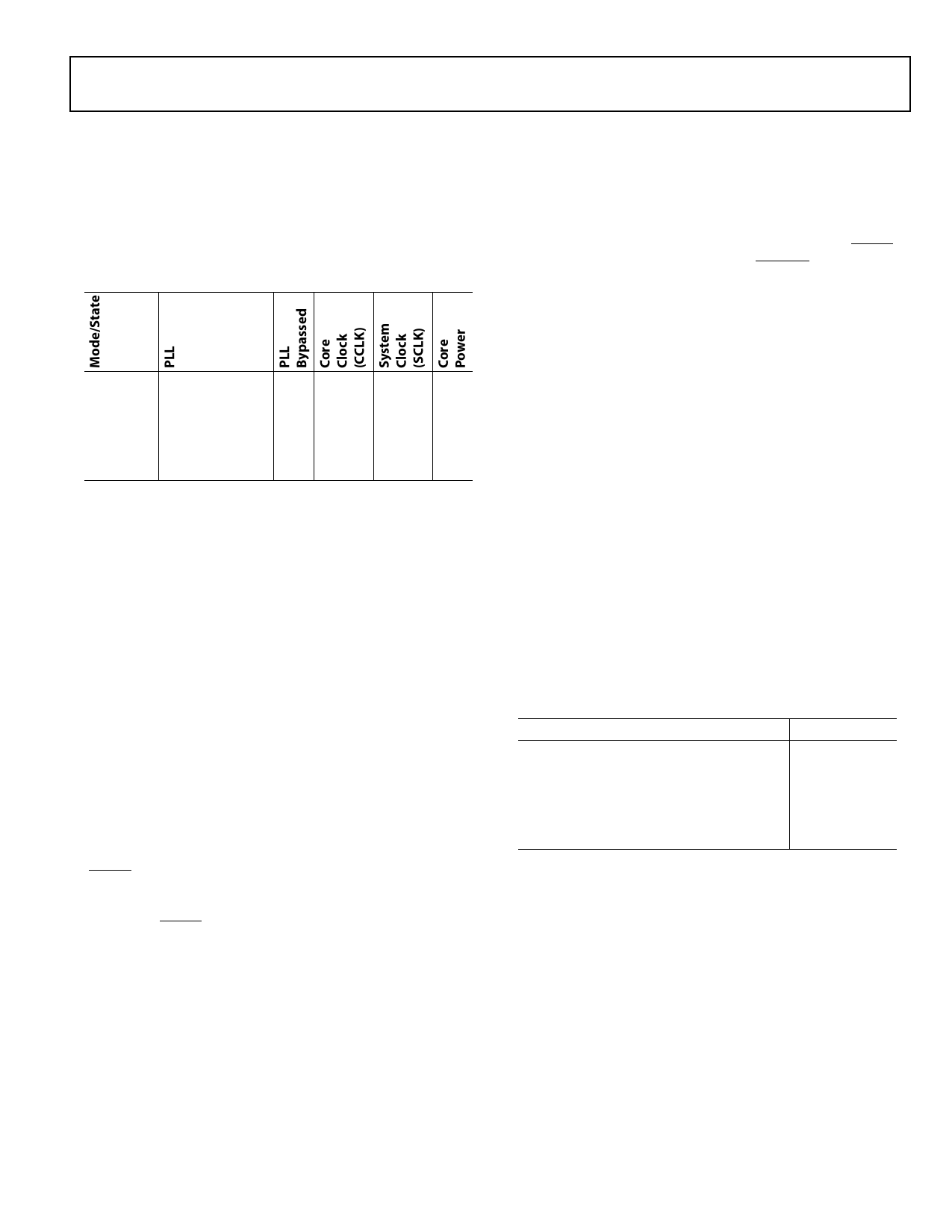
| |||
ADSP-BF539/ADSP-BF539F
The VDDRTC should either be connected to an isolated supply
such as a battery (if the RTC is to operate while the rest of the
chip is powered down) or should be connected to the VDDEXT
plane on the board. The VDDRTC should remain powered when
the processor is in hibernate state and should also remain pow-
ered even if the RTC functionality is not being used in an
application. The MXEVDD should be connected to the VDDEXT
plane on the board at a single location with local bypass capaci-
tors. The MXEVDD should remain powered when the
processor is in hibernate state and should also remain powered
even when the MXVR functionality is not being used in an
application. The MPIVDD should be connected to the VDDINT
plane on the board at a single location through a ferrite bead
with local bypass capacitors.
The power dissipated by a processor is largely a function of the
clock frequency of the processor and the square of the operating
voltage. For example, reducing the clock frequency by 25%
results in a 25% reduction in dynamic power dissipation, while
reducing the voltage by 25% reduces dynamic power dissipation
by more than 40%. Further, these power savings are additive in
that, if the clock frequency and supply voltage are both reduced,
the power savings can be dramatic.
The dynamic power management feature of the
ADSP-BF539/ADSP-BF539F processors allow both the proces-
sor input voltage (VDDINT) and clock frequency (fCCLK) to be
dynamically controlled.
The savings in power dissipation can be modeled using the
power savings factor and % power savings calculations.
The power savings factor is calculated as
Power Savings Factor
where
=
-f--C---C---L--K---R--E---D--
fCCLKNOM
×
⎛
⎝
V-V----D-D--D-D--I-IN-N--T-T--N-R--OE---DM--⎠⎞
2
×
⎛
⎝
-T----R---E--D--
TNOM
⎞
⎠
fCCLKNOM is the nominal core clock frequency.
fCCLKRED is the reduced core clock frequency.
VDDINTNOM is the nominal internal supply voltage.
VDDINTRED is the reduced internal supply voltage.
TNOM is the duration running at fCCLKNOM.
TRED is the duration running at fCCLKRED.
The Power Savings Factor is calculated as
% Power Savings = (1 – Power Savings Factor) × 100%
VOLTAGE REGULATION
The Blackfin processor provides an on-chip voltage regulator
that can generate processor core voltage levels 1.0 V
(–5%/+10%) to 1.20 V (–5%/+10%) and 1.25 V (–4%/+10%)
from an external 2.7 V to 3.6 V supply. For operation below
2.7 V, an external voltage regulator must be used. Figure 6
shows the typical external components required to complete the
power management system.† The regulator controls the internal
† See Switching Regulator Design Considerations for ADSP-BF533 Blackfin
Processors (EE-228).
logic voltage levels and is programmable with the voltage regu-
lator control register (VR_CTL) in increments of 50 mV. To
reduce standby power consumption, the internal voltage regula-
tor can be programmed to remove power to the processor core
while I/O power (VDDRTC, MXEVDD, VDDEXT) is still supplied.
While in the hibernate state, I/O power is still being applied,
eliminating the need for external buffers. The voltage regulator
can be activated from this power-down state through an RTC
wake-up, a CAN wake-up, an MXVR wake-up, a general-pur-
pose wake-up, or by asserting RESET, all of which will then
initiate a boot sequence. The regulator can also be disabled and
bypassed at the user’s discretion.
2.25V TO 3.6V
INPUT VOLTAGE
RANGE
VDDEXT
(LOW-INDUCTANCE)
SET OF DECOUPLING
CAPACITORS
100nF
+
100µF
FDS9431A
10µF
LOW ESR
+
100µF
10µH
+
100µF
ZHCS1000
SHORT AND LOW-
INDUCTANCE WIRE
NOTE: DESIGNER SHOULD MINIMIZE
TRACE LENGTH TO FDS9431A.
VDDEXT
VDDINT
VROU T
VROU T
GND
Figure 6. Voltage Regulator Circuit
CLOCK SIGNALS
The ADSP-BF539/ADSP-BF539F processors can be clocked by
an external crystal, a sine wave input, or a buffered, shaped
clock derived from an external clock oscillator.
If an external clock is used, it should be a TTL-compatible signal
and must not be halted, changed, or operated below the speci-
fied frequency during normal operation. This signal is
connected to the processor’s CLKIN pin. When an external
clock is used, the XTAL pin must be left unconnected.
Alternatively, because the ADSP-BF539/ADSP-BF539F proces-
sors include an on-chip oscillator circuit, an external crystal can
be used. For fundamental frequency operation, use the circuit
shown in Figure 7 on Page 16. A parallel-resonant, fundamental
frequency, microprocessor-grade crystal is connected across the
CLKIN and XTAL pins. The on-chip resistance between CLKIN
and the XTAL pin is in the 500 kΩ range. Further parallel resis-
tors are typically not recommended. The two capacitors and the
series resistor, shown in Figure 7 on Page 16, fine tune the phase
and amplitude of the sine frequency. The capacitor and resistor
values, shown in Figure 7 on Page 16, are typical values only.
The capacitor values are dependent upon the crystal manufac-
turer’s load capacitance recommendations and the physical PCB
Rev. A | Page 15 of 60 | February 2008
Share Link: 