FDS4435A 데이터 시트보기 (PDF) - Fairchild Semiconductor
부품명
상세내역
제조사
FDS4435A Datasheet PDF : 5 Pages
| |||

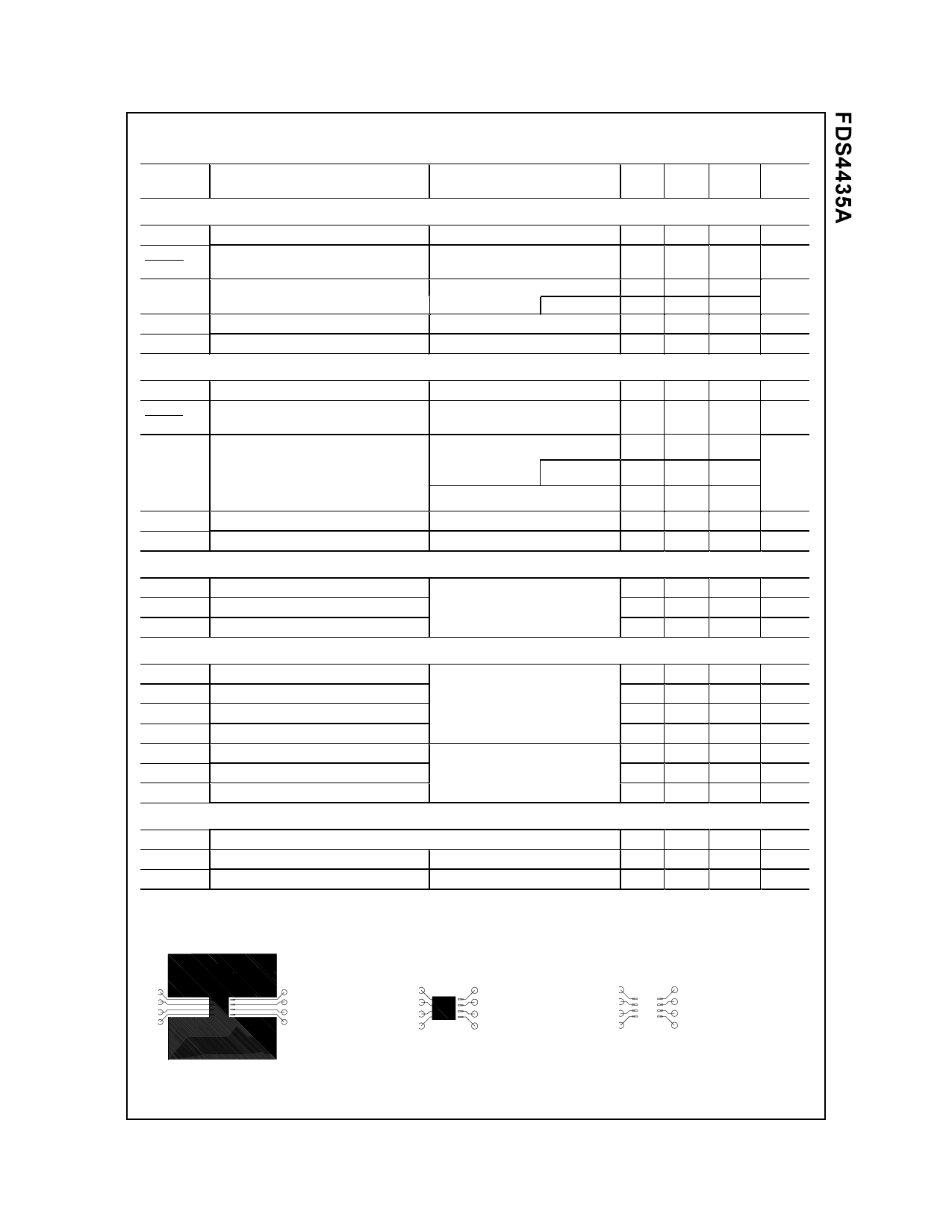
Electrical Characteristics
Symbol
Parameter
TA = 25°C unless otherwise noted
Test Conditions
Min Typ Max Units
Off Characteristics
BVDSS
Drain-Source Breakdown Voltage
VGS = 0 V, ID = -250 µA
-30
V
∆BVDSS
∆TJ
IDSS
Breakdown Voltage Temperature
Coefficient
Zero Gate Voltage Drain Current
ID = -250 µA,Referenced to 25°C
VDS = -24 V, VGS = 0
-26
mV/°C
-1
µA
IGSSF
TJ = 125°C
Gate-Body Leakage Current, Forward VGS = 20 V, VDS = 0 V
-10
100
nA
IGSSR
Gate-Body Leakage Current, Reverse VGS = -20 V, VDS = 0 V
-100 nA
On Characteristics (Note 2)
VGS(th)
Gate Threshold Voltage
∆VGS(th)
∆TJ
RDS(on)
Gate Threshold Voltage
Temperature Coefficient
Static Drain-Source On-Resistance
VDS = VGS, ID = -250 µA
-1 -1.7
ID = -250 µA,Referenced to 25°C
4.2
-2
V
mV/°C
VGS = -10 V, ID = -9 A
0.015 0.017 Ω
ID(on)
gFS
On-State Drain Current
Forward Transconductance
TJ = 125°C
0.021 0.030
VGS = -4.5 V, ID = -7 A
VGS = -10 V, VDS = -5 V
VDS = -10 V, ID = -9 A
0.023 0.025
-40
A
25
S
Dynamic Characteristics
Ciss
Input Capacitance
Coss
Output Capacitance
Crss
Reverse Transfer Capacitance
VDS = -15 V, VGS = 0 V
f = 1.0 MHz
2010
pF
590
pF
260
pF
Switching Characteristics
td(on)
Turn-On Delay Time
tr
Turn-On Rise Time
td(off)
Turn-Off Delay Time
tf
Turn-Off Fall Time
Qg
Total Gate Charge
Qgs
Gate-Source Charge
Qgd
Gate-Drain Charge
(Note 2)
VDD = -15 V, ID = -1 A
VGS = -10 V, RGEN = 6 Ω
VDS = -15 V, ID = -9 A
VGS = -5 V,
12
22
ns
15
27
ns
100 140
ns
55
80
ns
21
30
nC
6
nC
8
nC
Drain-Source Diode Characteristics and Maximum Ratings
IS
Maximum Continuous Drain-Source Diode Forward Current
-2.1
A
VSD
Drain-Source Diode Forward Voltage VGS = 0 V, IS = -2.1 A (Note 2)
0.75 -1.2
V
trr
Source-Drain Reverse Recovery Time IF = -10 A, dlF/dt = 100 A/µS
36
80
ns
Notes:
1: RqJA is the sum of the junction-to-case and case-to-ambient resistance where the case thermal reference is defined as the solder mounting surface of the
drain pins. RqJC is guaranteed by design while RqCA is determined by the user's board design.
a) 50° C/W when
mounted on a 1 in2
pad of 2 oz. copper.
b) 105° C/W when
mounted on a 0.04 in2
pad of 2 oz. copper.
c) 125° C/W when mounted
on a minimum pad.
Scale 1 : 1 on letter size paper
2: Pulse Test: Pulse Width £ 300 ms, Duty Cycle £ 2.0%
FDS4435A Rev. D