RMBA19500-58 데이터 시트보기 (PDF) - Raytheon Company
부품명
상세내역
제조사
RMBA19500-58 Datasheet PDF : 4 Pages
| |||
RMBA19500-58 - PCS 2 Watt Linear GaAs
RF Components MMIC Power Amplifier
PRODUCT INFORMATION
Application
Information
CAUTION: THIS IS AN ESD SENSITIVE DEVICE.
The following describes a procedure for evaluating the RMBA19500-58, a monolithic high efficiency
power amplifier, in a surface mount package, designed for use as a driver stage for PCS Base station
or as the final output stage for Micro- and Pico-Cell base stations. Figure 1 shows the package outline
and the pin designations. Figure 2 shows the functional block diagram of the packaged product. The
RMBA19500-58 requires external passive components for DC bias and RF input/output matching
circuits. A recommended schematic circuit is shown in Figure 3. The gate biases for the three stages of
the amplifier may be set by simple resistive voltage dividers. Figure 4 shows a typical layout of an
evaluation board, corresponding to the schematic circuits of figure 3. The following designations should
be noted:
(1) Pin designations are as shown in figure 2.
(2) Vg1, Vg2 and Vg3 are the Gate Voltages
(negative) applied at the pins of the package
(3) Vgg1, Vgg2 and Vgg3 are the negative supply
voltages at the evaluation board terminals
(Vg1and Vg2 are tied together)
(4) Vd1, Vd2 and Vd3 are the Drain Voltages
(positive) applied at the pins of the package
(5) Vdd is the positive supply voltage at the
evaluation board terminal (Vd1, Vd2 and Vd3
are tied together)
Note: The base of the package must be soldered
on to a heat sink for proper operation.
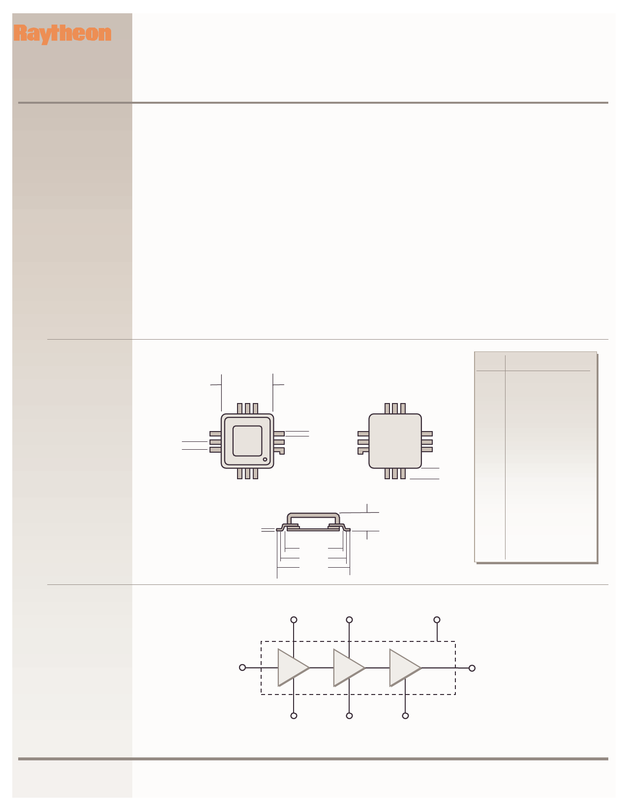
Figure 1
12 Lead Plastic Air
Cavity Package with
Integral Heat Sink
Dimensions in inches
TOP VIEW
BOTTOM VIEW
A
0.030
0.200 SQ.
6 54
45 6
7
8
3
RAY
RMBA
2
3
0.015
2
13
7
8
19500
9
1
1
9
10
12
11
12
10 0.041
11
PLASTIC LID
0.010
0.230
0.246
0.282
0.075 MAX.
SIDE SECTION
Pin # Description
1 RF Out & Vd3
2 RF Out & Vd3
3 RF Out & Vd3
4 VD1
5 GND
6 VG1
7 RF In
8 GND
9 VG2
10 VD2
11 GND
12 VG3
13 GND
Figure 2
Functional Block
Diagram of
Packaged Product
Vd1
Pin# 4
Vd2
Pin# 10
GND
Pin# 5, 8, 11, 13
RF IN
Pin# 7
RF OUT & Vd3
Pin# 1, 2, 3
Vg1
Pin# 6
Vg2
Pin# 9
Vg3
Pin# 12
www.raytheonrf.com
Specifications are based on most current or latest revision.
Revised June 27, 2003
Page 2
Raytheon RF Components
362 Lowell Street
Andover, MA 01810
Share Link: 