UPC8139GR-7JH 데이터 시트보기 (PDF) - NEC => Renesas Technology
부품명
상세내역
제조사
UPC8139GR-7JH Datasheet PDF : 20 Pages
| |||
µPC8139GR-7JH
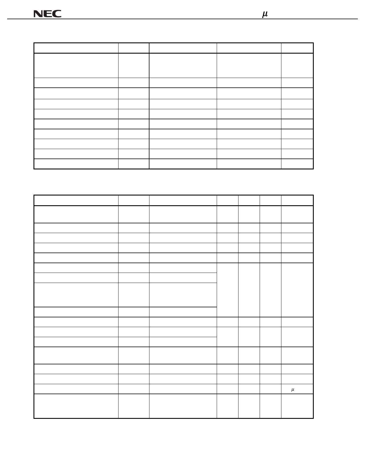
ABSOLUTE MAXIMUM RATINGS
Parameter
Symbol
Condition
Rating
Unit
Power supply voltage
VCC
Pins 5, 7, 12, 13, 19, 25,
4.5
V
29, 30
TA = +25°C
Power save pin voltage
VPS
Pin 23, Pin 24, TA = +25°C
4.5
V
Power dissipation
PD
Note
TA = +80°C
TBD
mW
Operating ambient temperature
TA
–30 to +80
°C
Storage temperature
Tstg
–55 to +150
°C
Pin current of Pin 8
I8 pin
4
mA
Pin current of Pin 10
I10 pin
4
mA
Collector to base voltage in VCO
VCBO
Pin 12 → Pin 11
4.5
V
Collector to emitter voltage in VCO VCEO
Pin 12 → Pin 10
4.5
V
Emitter to base voltage in VCO
VEBO
Pin 10 → Pin 11
3.0
V
Note When mounted on 50 × 50 × 1.6 mm double sided copper clad epoxy glass board
RECOMMENDED OPERATING RANGE
Parameter
Symbol
Power supply voltage
VCC
Power save pin voltage
Operating ambient temperature
TX up converter output frequency
TX up converter LO input frequency
TX up converter input frequency
IQ-MOD output frequency
2nd VCO oscillating frequency
(IQ-MOD LO, 2nd MIX LO input
frequency)
2nd MIX input frequency
2nd MIX output frequency
2nd IF amplifier input frequency
2nd IF amplifier output frequency
I/Q input frequency
VPS
TA
fTX • MIXout
fTX • MIX-LOin
fTX • MIXin
fMODout
f2ndVCO
(fMOD • LOin,
f2ndMIX-LOin)
f2ndMIXin
f2ndMIXout
f2ndIFin
f2ndIFout
fI/Qin
TX up converter LO input level
2nd MIX input level
2nd IF amplifier input level
I/Q input amplitude
PTX • MIX-LOin
P2ndMIXin
P2ndIFin
VI/Qin
Condition
Pins 5, 7, 12, 13, 19, 25,
29, 30
Pin 23, Pin 24
PTX • MIX-LOin = –10 dBm
VI/Qin = 600 mVP-P (MAX.),
Double phase
Double phase input
I/Q (DC) = Ib/Qb (DC) =
VCC/2
MIN.
2.7
TYP.
3.0
MAX.
4.0
0
–
VCC
–30
+25
+80
1800
–
2000
1500
–
1800
220
–
270
Unit
V
V
°C
MHz
MHz
MHz
8
10.8
12
8
10.8
12
MHz
MHz
DC
–
10
MHz
–15
–10
–5
dBm
–90
–
–10
dBm
23
–
108 dBµ VEMF
–
500
600
mVP-P
4
Preliminary Data Sheet
Share Link: 