M52342SP 데이터 시트보기 (PDF) - MITSUBISHI ELECTRIC
부품명
상세내역
제조사
M52342SP Datasheet PDF : 14 Pages
| |||
MITSUBISHI ICs (TV)
M52342SP
PLL-SPLIT VIF/SIF IC
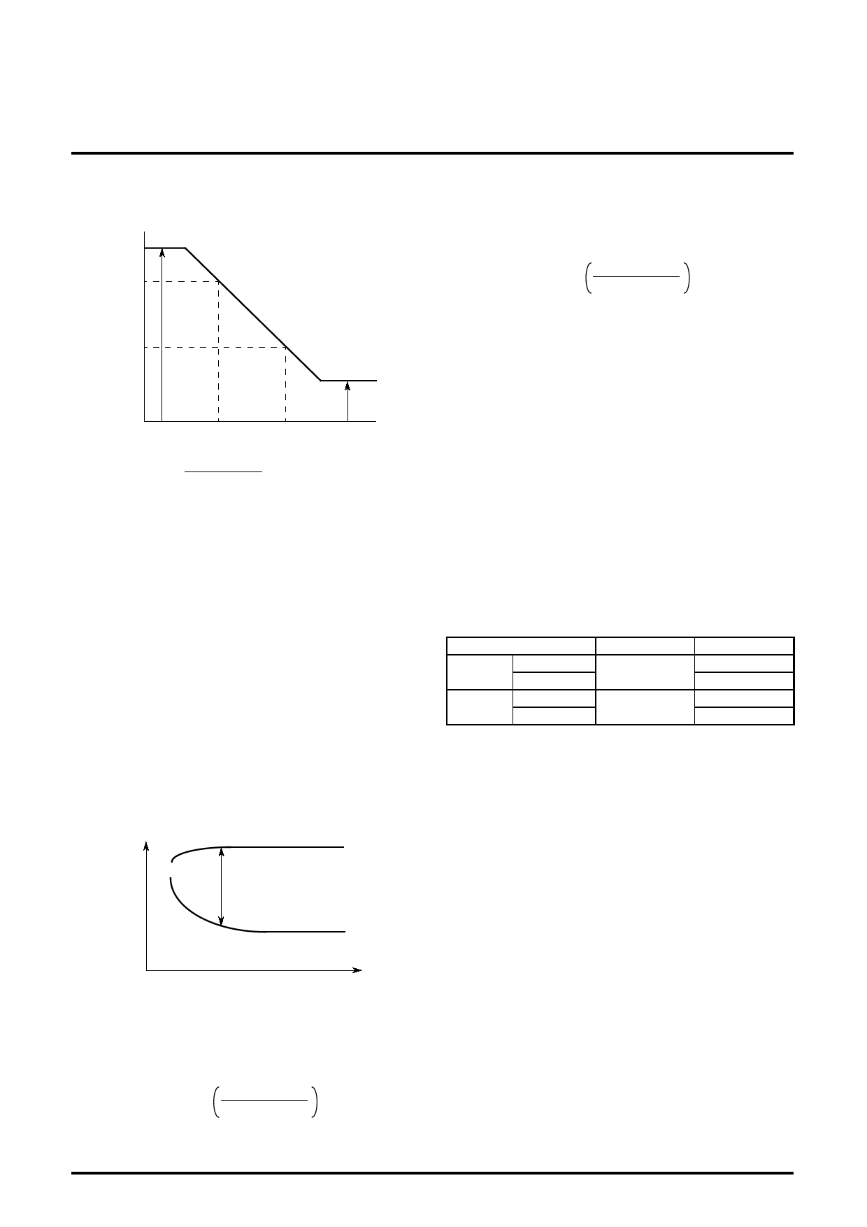
3. IN the graph, maximum and minimum DC voltage are V2H and
V2L, respectively.
TP2
Voltage
3V
V2H
2V
V2L
f (3)
f (2)
f (MHz)
1000 (mV)
µ=
f (2) - f (3) (kHz)
(mV/kHz)
IM Intermodulation
1. Input SG11 into VIF IN, and measure EQ output TP18A with an
oscilloscope.
2. Adjust AGC filter voltage V8 so that the minimum DC level of the
output waveform is 1.0V.
3. At this time, measure, TP18A with a spectrum analyzer.
The intermodulation is defined as a difference between 920kHz
and 3.58MHz frequency components.
LIM Limiting sensitivity
1. Input SG17 (SG22) into SIF input, and measure the 400Hz
component level of AF output TP10.
2. Input SG19 (SG24) into SIF input, and measure the 400Hz
component level of AF output TP10.
3. The input limiting sensitivity is defined as the input level when a
difference between each 400Hz components of audio output
(TP10) is 30dB, as shown below.
Audio output
(mVrms)
30dB
Audio output while
SG17 (SG22) is input
Audio output while
SG19 (SG24) is input
AF S/N
1. Input SG20 (SG25) into SIF input, and measure the output noise
level of AF output TP1. This level is named VN.
2. S/N is;
VoAF (mVr.m.s)
S/N=20log VN (mVr.m.s) (dB)
CQIF QIF control
Lower the voltage of V7, and measure the voltage of V7 when DC
voltage of TP13 begins to change.
THE NOTE IN THE SYSTEM SETUP
M52342SP has 2 power supply pins of Vcc (pin 14) and Vreg. OUT
(pin 17). Pin 14 is for AFT output, RF AGC output circuits and 5V
regulated power circuit and Pin 17 is for the other circuit blocks.
In case M52342SP is used together with other ICs like VIF
operating at more than 5V, the same supply voltage as that of
connected ICs is applied to VCC and Vreg. Out is opened. The other
circuit blocks, connected to Vreg. OUT are powered by internal 5V
regulated power supply.
In case the connecting ICs are operated at 5V, 5V is supplied to
both VCC and Vreg.OUT.
LOGIC TABLE
10k “H”
10k “L”
20k “H”
20k “L”
20k “H”
20k “L”
AF
NTSC
PAL
AFT
DEFEAT
NORMAL
DEFEAT
NORMAL
(dBµ) SIF input
AMR AM Rejection
1. Input SG18 (SG23) into SIF input, and measure the output level
of AF output TP10. This level is named VAM.
2. AMR is;
VoAF (mVr.m.s)
AMR=20log
(dB)
VAM (mVr.m.s)
5
Share Link: 