SP9600JN 데이터 시트보기 (PDF) - Signal Processing Technologies
부품명
상세내역
제조사
SP9600JN Datasheet PDF : 9 Pages
| |||
0
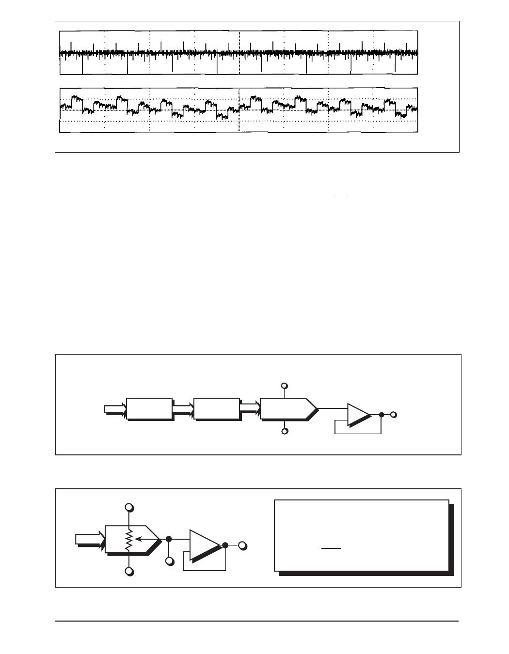
DNLE, INLE Plots
CODE
USING THE SP9600
External Reference
The R-2R DAC input resistance is code depen-
dent and is minimum (11kΩ) at code 1365 and
2731. And, it is nearly infinite at code 0. Because
of the code-dependent nature of the reference
inputs, a high quality, low output impedance
amplifier should be used to drive the V and
REF
AGND inputs.
Serial Clock and Update Rate
The SP9600 maximum serial clock rate (SCLK)
is given by 1/(tCH+tCL) which is approximately
12.5 MHz. The digital word update rate is limited
by the chip select period, which is 12 X SCLK
+0.5 lsb
DNLE
-0.5 lsb
+0.5 lsb
INLE
-0.5 lsb
4095
periods plus the CS high pulse width tCSW. This
is equal to a 1 µs or 1 MHz update rate. However,
the DAC settling time to 12–Bits is 20 µs, which
for full scale output transitions would limit the
update rate to 50 kHz.
Logic Interface
The SP9600 is designed to be compatible with
TTL and CMOS logic levels. However, driving
the digital inputs with TTL level signals will
increase the power consumption of the part by
300 µA. In order to achieve the lowest power
consumption use rail-to-rail CMOS levels to
drive the digital inputs.
DIN
1
SHIFT
REGISTER
DDAACC
RREEGGISTTEERR
12 LATCH
12
VREF
DAC
AGND
+
–
VOUT
Figure 1. Detailed Block Diagram
VREF
DIN
+
–
AGND
Figure 2. Transfer Function
VDAC
WHERE…
VOUT
VOUT = VDAC
( ) VDAC =
DIN
4096
x (VREF - AGND) + AGND
SP9600DS/04
SP9600 12-Bit, Low Power Voltage Output D/A Converter
5
© Copyright 2000 Sipex Corporation
Share Link: 