VRE410L 데이터 시트보기 (PDF) - Thaler Corporation
부품명
상세내역
제조사
VRE410L Datasheet PDF : 20 Pages
| |||
DISCUSSION OF PERFORMANCE
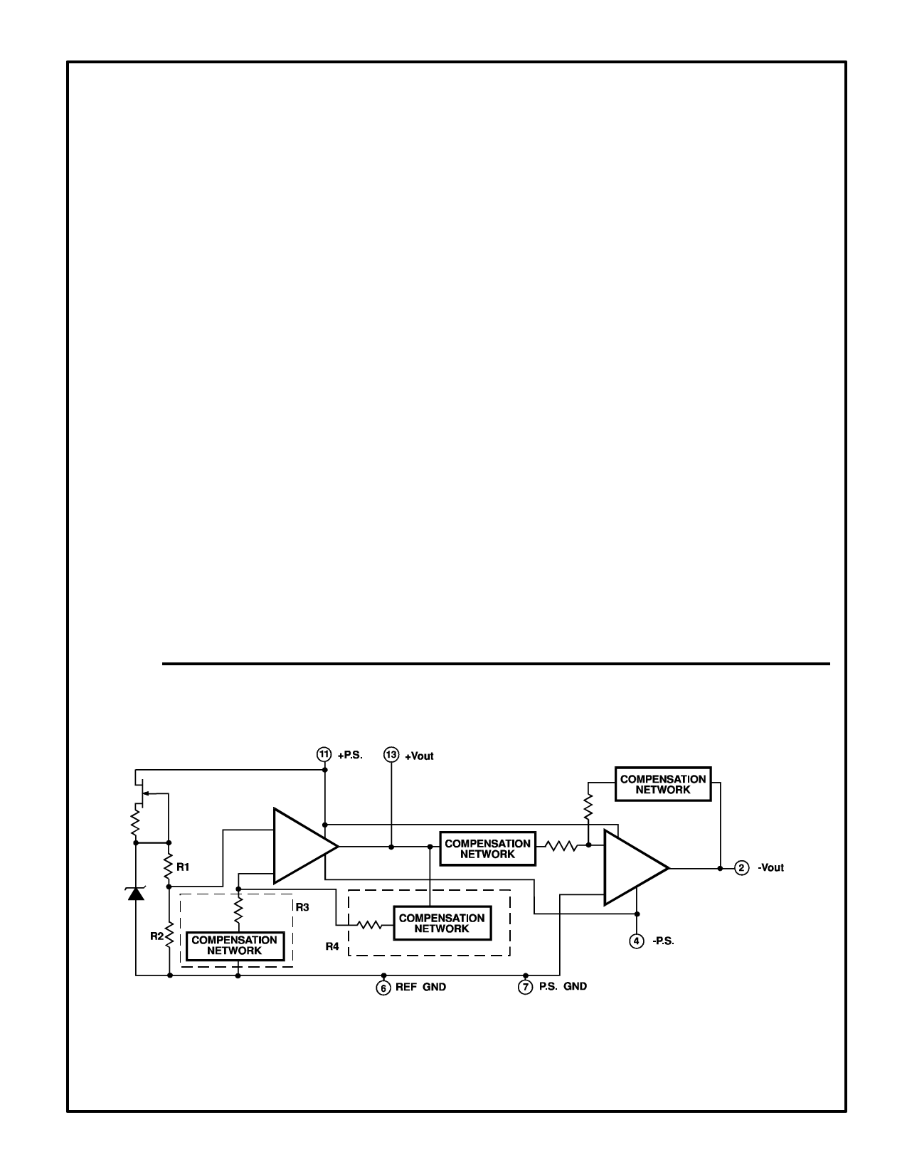
THEORY OF OPERATION
The following discussion refers to the schematic in
figure 2 below. A FET current source is used to bias
a 6.3V zener diode. The zener voltage is divided by
the resistor network R1 and R2. This voltage is then
applied to the noninverting input of the operational
amplifier which amplifies the voltage to produce a
4.500V output. The gain is determined by the
resistor networks R3 and R4: G=1 + R4/R3. The
6.3V zener diode is used because it is the most
stable diode over time and temperature.
The current source provides a closely regulated
zener current, which determines the slope of the
references’ voltage vs. temperature function. By
trimming the zener current a lower drift over
temperature can be achieved. But since the voltage
vs. temperature function is nonlinear this
compensation technique is not well suited for wide
temperature ranges.
Thaler Corporation has developed a nonlinear
compensation network of thermistors and resistors
that is used in the VRE series voltage references.
This proprietary network eliminates most of the
nonlinearity in the voltage vs. temperature function.
By adjusting the slope, Thaler Corporation produces
a very stable voltage over wide temperature ranges.
This network is less than 2% of the overall network
resistance so it has a negligible effect on long term
stability.
The VRE404 reference has it’s ground brought out
on two pins (pin 6 and 7) which are connected
internally. This allows the user to achieve greater
accuracy when using a socket. Voltage references
have a voltage drop across their power supply
ground pin due to quiescent current flowing through
the contact resistance. If the contact resistance was
constant with time and temperature, this voltage
drop could be trimmed out. When the reference is
plugged into a socket, this source of error can be as
high as 20ppm. By connecting pin 7 to the power
supply ground and pin 6 to a high impedance
ground point in the measurement circuit, the error
due to the contact resistance can be eliminated. If
the unit is soldered into place, the contact
resistance is sufficiently small that it does not effect
performance.
VRE404
FIGURE 2
VRE404DS REV. A MAY 1996
Share Link: 