139RPFB(2001) 데이터 시트보기 (PDF) - MAXWELL TECHNOLOGIES
부품명
상세내역
제조사
139RPFB Datasheet PDF : 9 Pages
| |||
Quad Comparators, Low Offset Voltage
139
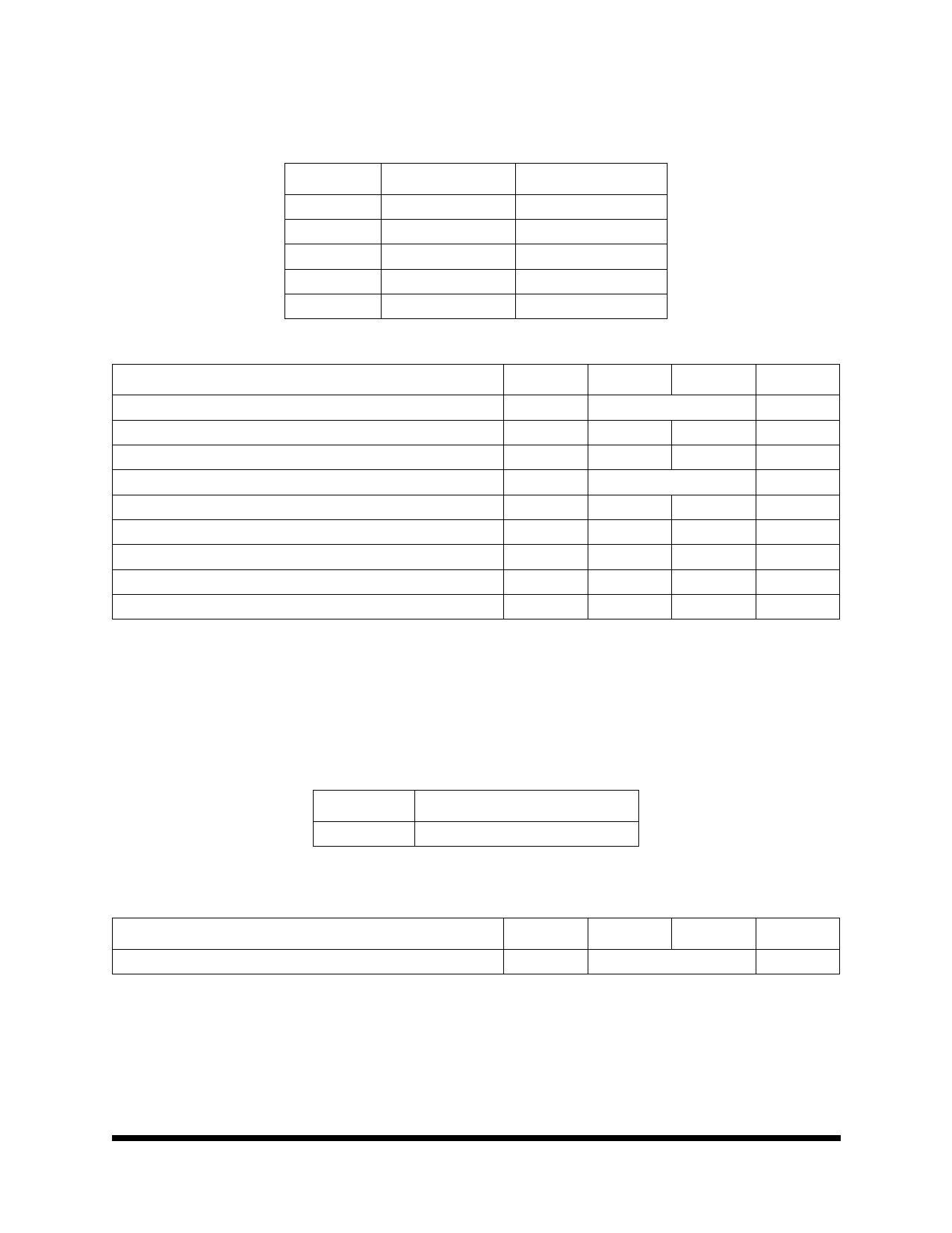
TABLE 1. PINOUT DESCRIPTION
PIN
SYMBOL
DESCRIPTION
2, 1, 14, 13
4, 6, 8, 10
5, 7, 9, 11
3
12
OUTPUT1 - 4
INPUT1- – 4
INPUT+ – 4
V+
GND
Output Signal
Negative Input Signal
Positive Input Signal
Positive Voltage
Ground
TABLE 2. 139 ABSOLUTE MAXIMUM RATINGS
PARAMETER
SYMBOL
MIN
MAX
UNIT
Supply Voltage (V+ - V-)
Differential Input Voltage1
V+ - V-
36 VDC or ±18 VDC
V
--
36
V
Input Voltage
-0.3
+36
V
Open Short-Circuit to Ground2
Continuous
Input Current (VIN < -0.3VDC)
--
50
mA
Power Dissipation
PD
--
1
W
Storage Temperature Range
TS
-65
150
°C
Operating Temperature Range
TA
-55
125
°C
ESD Tolerance 3
--
600
V
1. Positive excursions of input voltage may exceed the power supply level. As long as the other voltage remains within the com-
mon-mode range, the comparator will provide a proper output state. The low output voltage state must not be less than -0.3
VDC (or 0.3 VDC below the magnitude of the negative power supply, if used) (at 25°C).
2. Short Circuits from the output to V+ can cause excessive heating and eventual destruction. When considering short circuits to
ground, the maximum output current is ~20mA independent of the magnitude of V+.
3. 1.5 kΩ in series with 100 pF.
TABLE 3. DELTA LIMITS
PARAMETER
VARIATION
ICC
±10% of specified value in Table 5
Supply Voltage
TABLE 4. 139 RECOMMENDED OPERATING CONDITIONS
PARAMETER
SYMBOL
MIN
MAX
UNIT
V+ - V-
36 VDC or ±18 VDC
V
1000522
12.13.01 Rev1
All data sheets are subject to change without notice 2
©2001 Maxwell Technologies
All rights reserved.
Share Link: 