MC33304P 데이터 시트보기 (PDF) - Motorola => Freescale
부품명
상세내역
제조사
MC33304P Datasheet PDF : 12 Pages
| |||
MC33304
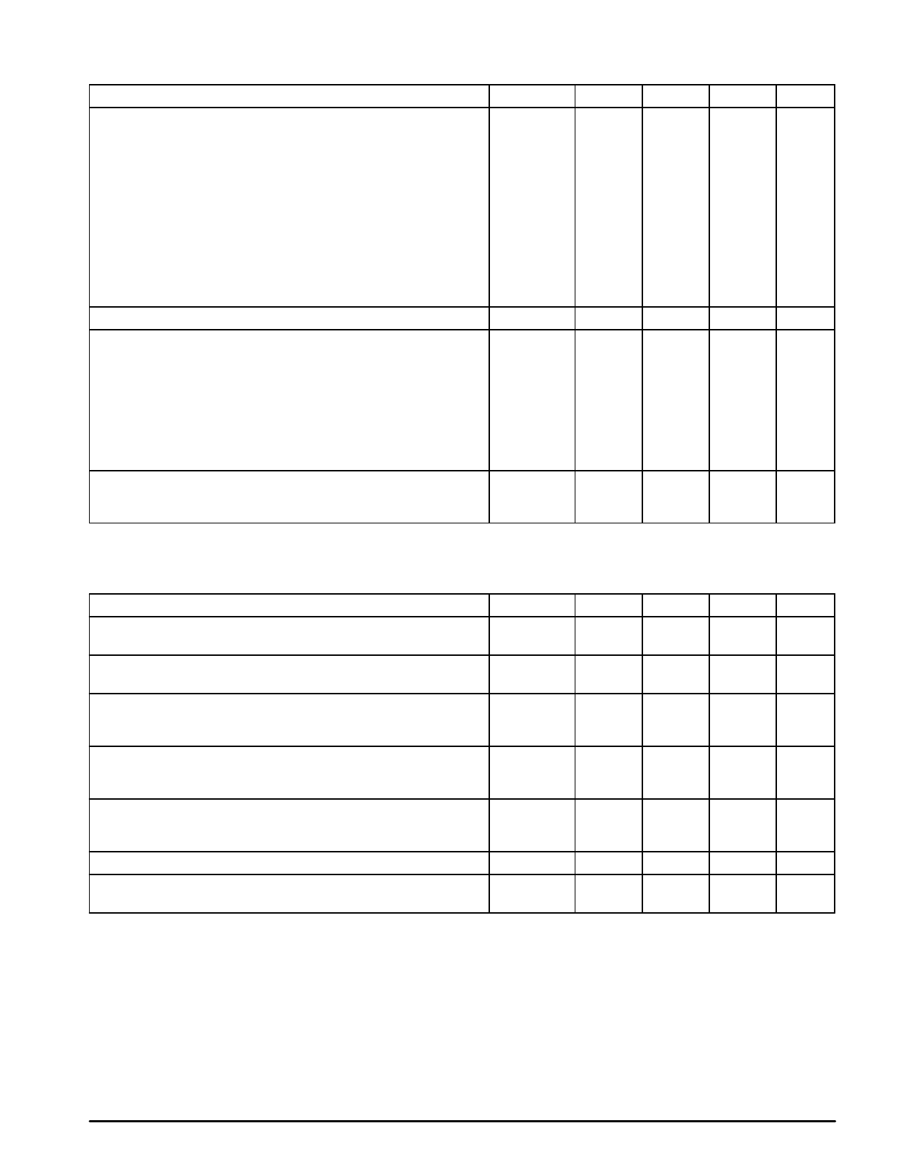
DC ELECTRICAL CHARACTERISTICS (continued) (VCC = +5.0 V, VEE = Gnd, TA = 25°C, unless otherwise noted.)
Characteristic
Symbol
Min
Typ
Max
Output Voltage Swing (VID = ±0.2 V)
Sleepmode
VCC = +5.0 V, VEE = 0 V, RL = 1.0 MΩ
VCC = 0 V, VEE = –5.0 V, RL = 1.0 MΩ
VCC = +2.0 V, VEE = 0 V, RL = 1.0 MΩ
VCC = 0 V, VEE = –2.0 V, RL = 1.0 MΩ
Awakemode
VCC = +5.0 V, VEE = 0 V, RL = 600 Ω
VCC = 0 V, VEE = –5.0 V, RL = 600 Ω
VCC = +2.0 V, VEE = 0 V, RL = 600 Ω
VCC = 0 V, VEE = –2.0 V, RL = 600 Ω
VCC = +2.5 V, VEE = –2.5 V, RL = 600 Ω
VCC = +2.5 V, VEE = –2.5 V, RL = 600 Ω
VOH
VOL
VOH
VOL
VOH
VOL
VOH
VOL
VOH
VOL
4.90
4.97
–
–
–4.96
–4.90
1.90
1.98
–
–
–1.97
–1.90
4.75
4.86
–
–
–4.85
–4.75
1.85
1.91
–
–
–1.90
–1.85
–
2.41
–
–
–2.40
–
Common Mode Rejection Ratio
CMRR
60
90
–
Power Supply Current (per Amplifier)
Sleepmode
VCC = +2.0 V, VEE = 0 V
VCC = +2.5 V, VEE = –2.5 V
VCC = +12 V, VEE = 0 V
Awakemode
TA = +25°C
TA = +25°C
TA = –40° to +105°C
TA = +25°C
VCC = +2.5 V, VEE = –2.5 V TA = +25°C
TA = –40° to +105°C
ID
–
85
–
–
110
140
–
–
150
–
125
–
–
1200
1625
–
–
1750
Thermal Resistance
SOIC
Plastic DIP
θJA
–
145
–
–
75
–
Unit
V
dB
µA
°C/W
AC ELECTRICAL CHARACTERISTICS (VCC = +6.0 V, VEE = –6.0 V, RL = 600 Ω, TA = 25°C, unless otherwise noted.)
Characteristic
Symbol
Min
Typ
Max
Slew Rate (VCC = +2.5 V, VEE = –2.5 V, AV = +1.0) (Note 6)
Awakemode
SR
0.5
0.89
–
Gain Bandwidth Product (f = 100 kHz)
Awakemode
GBW
–
2.2
–
Gain Margin (CL = 0 pF)
Awakemode
Sleepmode (RL = 1.0 kΩ)
Phase Margin (RL = 1.0 kΩ, VO = 0 V, CL = 0 pF)
Awakemode
Sleepmode
Am
–
6.0
–
–
9.0
–
φm
–
40
–
–
60
–
Sleepmode to Awakemode Transition Time
RL = 600 Ω
RL = 10 k
Awakemode to Sleepmode Transition Time
Channel Separation (f = 1.0 kHz)
Awakemode
ttr1
–
4.0
–
–
12
–
ttr2
–
1.5
–
CS
–
100
–
Unit
V/µs
MHz
dB
Deg
µsec
sec
dB
NOTES: 1. The differential input voltage of each amplifier is limited by two internal diodes. The diodes are connected across the inputs in parallel and opposite to
each other. For more differential input voltage range, use current limiting resistors in series with the input pins.
2. The common–mode input voltage range of each amplifier is limited by diodes connected from the inputs to both power supply rails. Therefore, the
voltage on either input must not exceed supply rail by more than ±500 mV.
3. Simultaneous short circuits of two or more amplifiers to the positive or negative rail can exceed the power dissipation ratings and cause eventual
failure of the device.
4. Rail–to–rail performance is achieved at the input of the amplifier by using parallel NPN–PNP differential stages. When the inputs are near the
negative rail (VEE < VCM < 800 mV), the PNP stage is on. When the inputs are above 800 mV (i.e. 800 mV < VCM < VCC), the NPN stage is on.
This switching of the input pairs will cause a reversal of input bias current. Slight changes in the input offset voltage will be noted between the NPN
and PNP pairs. Cross–coupling techniques have been used to keep this change to a minimum.
5. Power dissipation must be considered to ensure maximum junction (TJ) is not exceeded. (See Figure 2)
6. When connected as a voltage follower and used in transient conditions, a current limiting resistor may be needed between the output and the
inverting input. This is because of the back to back diodes clamped across the inputs. The value of this resistor should be between 1.0 kΩ and
10 kΩ. If the amplifier does not become slew rate limited and is processing low frequency waveforms, then no resistor would be necessary.
(The output could be tied directly to the negative input.)
MOTOROLA ANALOG IC DEVICE DATA
3
Share Link: 