SY605JCTR 데이터 시트보기 (PDF) - Micrel
부품명
상세내역
제조사
SY605JCTR Datasheet PDF : 8 Pages
| |||
Micrel
SY605
PIN DESCRIPTION
D0 – D7
Data input pins (ECL compatible). On the falling edge of
WRITE, D0 - D7 are latched into the DAC input register. D0
is the LSB. These inputs specify the amount of delay from the
rising edge of TRIG to the output pulse.
WRITE, WRITE
Differential write inputs (ECL compatible). These inputs
control the parallel data input latch. When WRITE is a logical
one, the data latch is transparent. Data is latched on the falling
edge of WRITE. A single-ended write may be used by
connecting WRITE to VBB.
OUT, OUT
Differential outputs (ECL compatible).
IEXT
Current reference pin. The amount of current sourced into this
pin determines the span of output delay. The voltage at IEXT
is typically –1.25V.
COMP1, COMP2
Compensation pins. A 0.1µF ceramic capacitor must be
connected between COMP1 and VEE0, and COMP2 and VEE0
(see Figure 3).
CE
Chip enable input (ECL compatible). CE must be a logical
zero on the rising edge of TRIG to enable the device to
respond to the trigger. If CE is floating, the trigger will always
be enabled.
VEE
Device power. All VEE pins must be connected.
VCC
Device ground. All VCC pins must be connected together.
TRIG, TRIG
Differential trigger inputs (ECL compatible). The rising edge
of TRIG is used to trigger the delay cycle if CE is a logical zero.
If CE is a logical one, no operation occurs. It is recommended
that triggering be performed with differential inputs.
VBB
A –1.36V (typical) output.
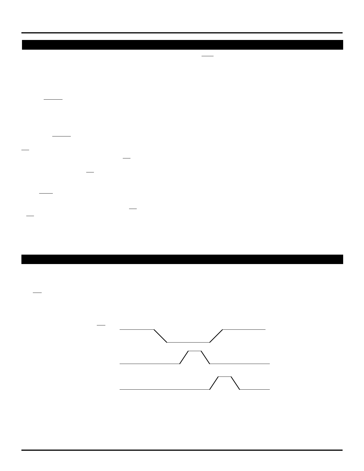
FUNCTIONAL DESCRIPTION
The output pulse generation cycle begins with the arrival of
TRIG shown in Figure 1. The DAC values are latched by the
rising edge of WRITE. Then, when TRIG transitions to a high
and CE is low the linear ramp is initiated.
When the ramp level reaches that of the DAC, the
comparator initiates the pulse generator to produce an output
pulse resets the ramp and the cycle is ready to begin again.
CE
TRIG
OUT
Figure 1.
2
Share Link: 