EL2257C 데이터 시트보기 (PDF) - Elantec -> Intersil
부품명
상세내역
제조사
EL2257C Datasheet PDF : 21 Pages
| |||
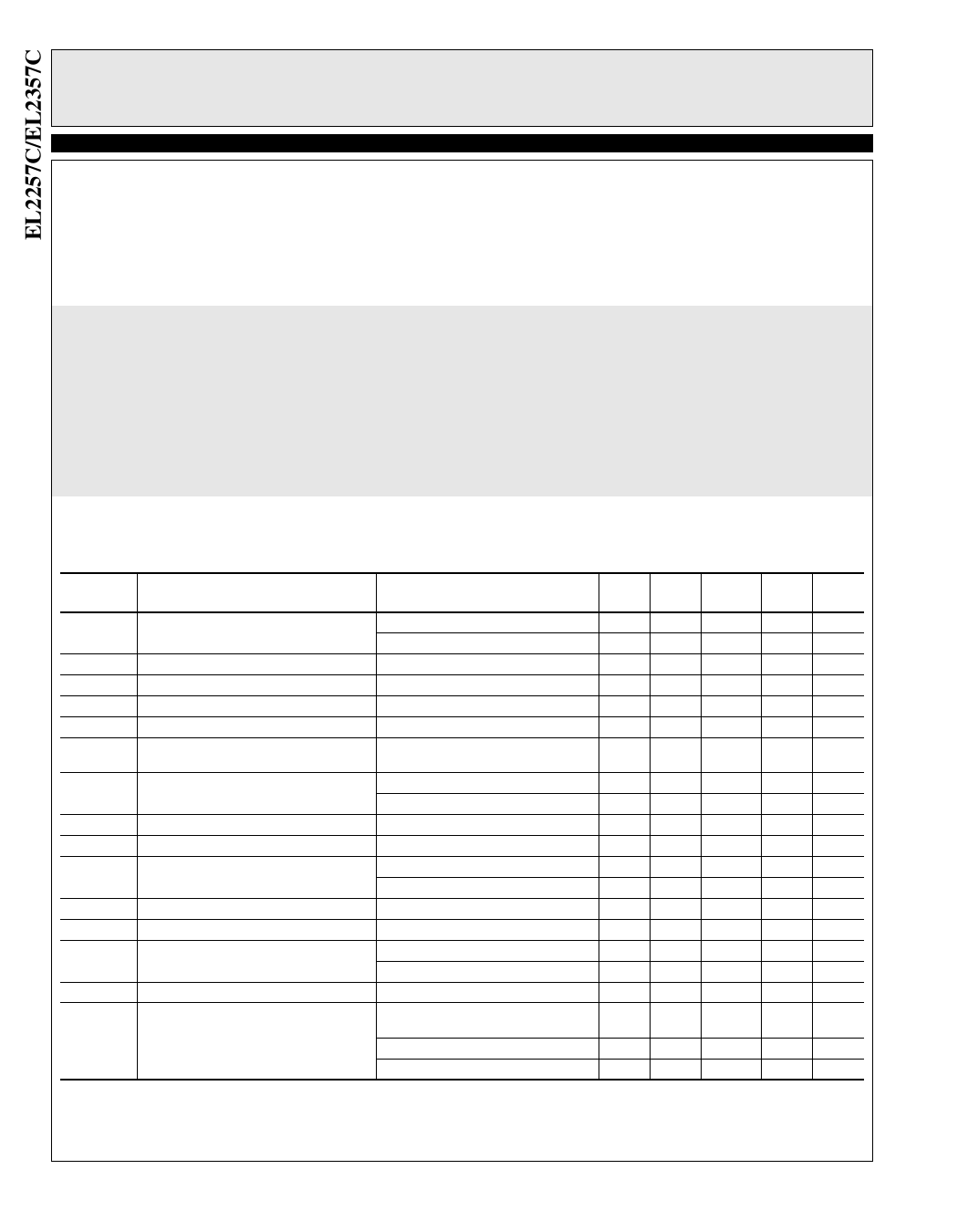
EL2257C/EL2357C
125 MHz Single Supply, Clamping Op Amps
Absolute Maximum Ratings (TA = 25 °C)
Supply Voltage between VS and GND
Input Voltage (IN+, IN-, ENABLE, CLAMP)
Differential Input Voltage
12.6V
GND–0.3V, VS+0.3V
±6V
Maximum Output Current
Output Short Circuit Duration
90 mA
(see note [1] DC Electrical Characteristics)
Power Dissipation
Storage Temperature Range
Ambient Operating Temperature Range
Operating Junction Temperature
See Curves
-65°C to +150°C
-40°C to +85°C
150°C
Important Note:
All parameters having Min/Max specifications are guaranteed. The Test Level column indicates the specific device testing actually performed during
production and Quality inspection. Elantec performs most electrical tests using modern high-speed automatic test equipment, specifically the LTX77
Series system. Unless otherwise noted, all tests are pulsed tests, therefor TJ = TC = TA.
Test Level Test Procedure
I
100% production tested and QA sample tested per QA test plan QCX0002.
II
100% production tested at TA = 25°C and QA sample tested at TA = 25°C, TMAX and TMIN per QA test plan QCX0002.
III
QA sample tested per QA test plan QCX0002.
IV
Parameter is guaranteed (but not tested) by Design and Characterization Data.
V
Parameter is typical value at TA = 25°C for information purposes only.
DC Electrical Characteristics
VS=+5V, GND=0V, TA=25°C, VCM=1.5V, VOUT=1.5V, VCLAMP=+5V, VENABLE=+5V, unless otherwise specified.
Parameter
Description
Test Conditions
Min Typ
VOS
Offset Voltage
EL2257C
-4
EL2357C
-6
TCVOS
IB
IOS
TCIOS
PSRR
CMRR
Offset Voltage Temperature Coefficient
Input Bias Current
Input Offset Current
Input Bias Current Temperature Coefficient
Power Supply Rejection Ratio
Common Mode Rejection Ratio
Measured from Tmin to Tmax
VIN=0V
VIN=0V
Measured from Tmin to Tmax
VS=VENABLE=+2.7V to +12V,
VCLAMP=OPEN
VCM=0V to +3.8V
10
-5.5
-1100 150
50
45
70
50
65
VCM=0V to +3.0V
55
70
CMIR
Common Mode Input Range
0
RIN
Input Resistance
CIN
Input Capacitance
Common Mode
SOIC Package
PDIP Package
1
2
1
1.5
ROUT
IS,ON
IS,OFF
PSOR
Output Resistance
Supply Current - Enabled (per amplifier)
Supply Current - Shut Down (per amplifier)
Power Supply Operating Range
Av=+1
VS=VCLAMP=+12V, VENABLE=+12V
VS=VCLAMP=+10V, VENABLE=+0.5V
VS=VCLAMP=+12V, VENABLE=+0.5V
40
5
0
5
2.7
AVOL
Open Loop Gain
VS=VCLAMP=+12V, VOUT=+2V to +9V,
65
80
RL=1 kΩ to GND
VOUT=+1.5V to +3.5V, RL=1 kΩ to GND
70
VOUT=+1.5V to +3.5V, RL=150Ω to GND
60
Max
4
6
-10
+1100
Test
Level
I
I
V
I
I
V
I
Units
mV
mV
µV/°C
µA
nA
nA/°C
dB
I
dB
I
dB
VS-1.2
I
V
I
MΩ
V
pF
V
pF
V
mΩ
6.5
I
mA
50
I
µA
V
µA
12.0
I
V
I
dB
V
dB
V
dB
2
Share Link: 