MT28F002B3 데이터 시트보기 (PDF) - Micron Technology
부품명
상세내역
제조사
MT28F002B3 Datasheet PDF : 31 Pages
| |||
2Mb
SMART 3 BOOT BLOCK FLASH MEMORY
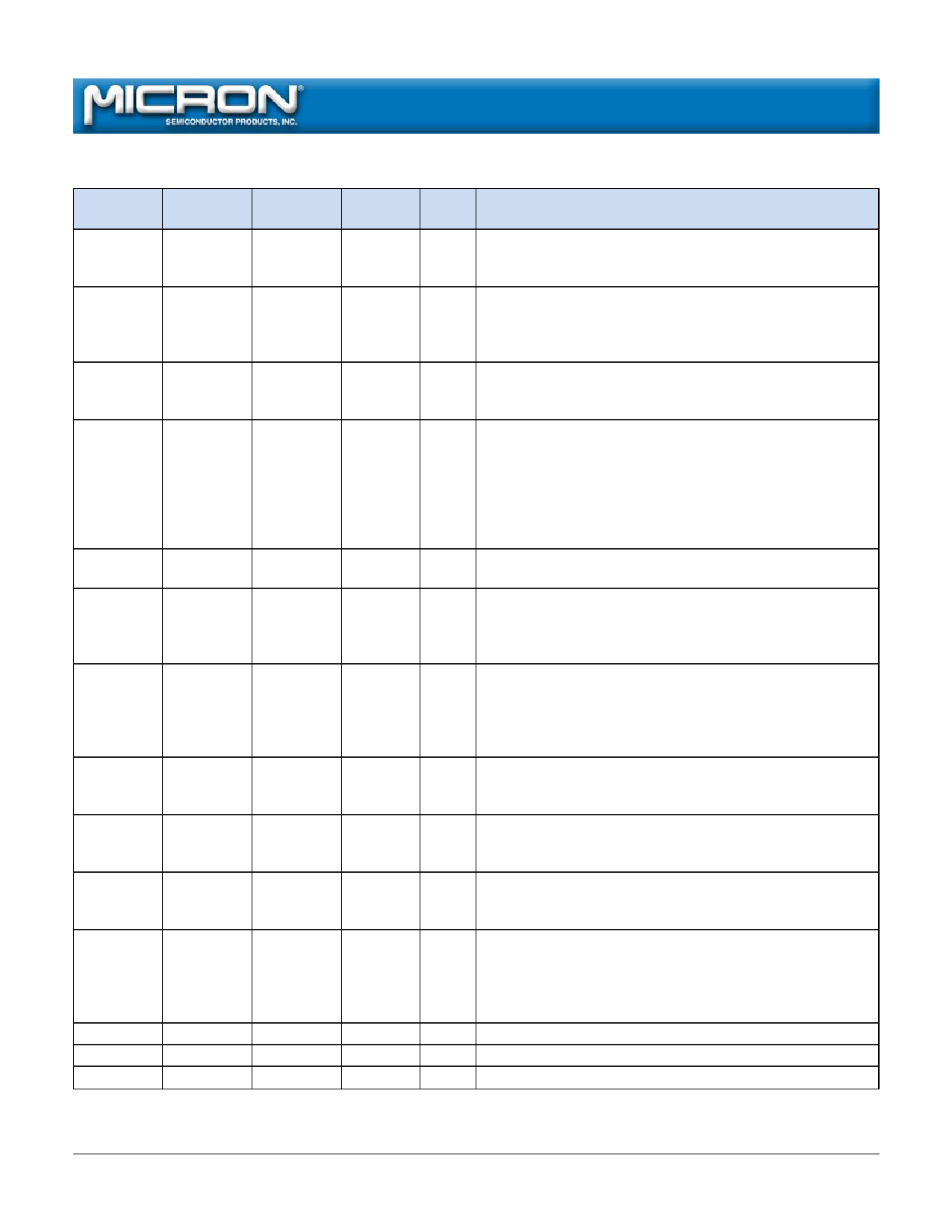
PIN DESCRIPTIONS
44-PIN SOP 40-PIN TSOP 48-PIN TSOP
NUMBERS NUMBERS NUMBERS SYMBOL TYPE
DESCRIPTION
43
9
11
WE# Input Write Enable: Determines if a given cycle is a WRITE cycle. If
WE# is LOW, the cycle is either a WRITE to the command
execution logic (CEL) or to the memory array.
2
12
14
WP# Input Write Protect: Unlocks the boot block when HIGH if VPP =
VPPH1 (3.3V), VPPH2 (5V) or VPPH3 (12V)1 and RP# = VIH during a
WRITE or ERASE. Does not affect WRITE or ERASE operation
on other blocks.
12
22
26
CE#
Input Chip Enable: Activates the device when LOW. When CE# is
HIGH, the device is disabled and goes into standby power
mode.
44
10
12
RP#
Input Reset/Power-Down: When LOW, RP# clears the status register,
sets the internal state machine (ISM) to the array read mode
and places the device in deep power-down mode. All inputs,
including CE#, are “Don’t Care,” and all outputs are High-Z.
RP# unlocks the boot block and overrides the condition of
WP# when at VHH (12V); RP# must be held at VIH during all
other modes of operation.
14
24
28
OE# Input Output Enable: Enables data output buffers when LOW.
When OE# is HIGH, the output buffers are disabled.
33
–
47
BYTE# Input Byte Enable: If BYTE# = HIGH, the upper byte is active through
DQ8-DQ15. If BYTE# = LOW, DQ8-DQ14 are High-Z, and all
data is accessed through DQ0-DQ7. DQ15/(A - 1) becomes the
least significant address input.
11, 10, 9, 8,
7, 6, 5, 4,
42, 41, 40,
39, 38, 37,
36, 35, 34
21, 20, 19,
18, 17, 16,
15, 14, 8, 7,
36, 6, 5, 4,
3, 2, 1, 40
25, 24, 23,
22, 21, 20,
19, 18, 8, 7,
6, 5, 4, 3, 2,
1, 48
A0-A16/
(A17)
Input
Address Inputs: Select a unique, 16-bit word or 8-bit byte. The
DQ15/(A - 1) input becomes the lowest order address when
BYTE# = LOW (MT28F200B3) to allow for a selection of an
8-bit byte from the 262,144 available.
31
–
45
DQ15/ Input/ Data I/O: MSB of data when BYTE# = HIGH. Address Input:
(A - 1) Output LSB of address input when BYTE# = LOW during READ or
WRITE operation.
15, 17, 19, 25-28, 32-35 29, 31, 33,
21, 24, 26,
35, 38, 40,
28, 30
42, 44
DQ0-DQ7 Input/ Data I/Os: Data output pins during any READ operation or
Output data input pins during a WRITE. These pins are used to input
commands to the CEL.
16, 18, 20,
–
30, 32, 34, DQ8-DQ14 Input/ Data I/Os: Data output pins during any READ operation or
22, 25, 27,
36, 39, 41,
Output data input pins during a WRITE when BYTE# = HIGH. These
29
43
pins are High-Z when BYTE# is LOW.
1
11
13
VPP Supply Write/Erase Supply Voltage: From a WRITE or ERASE CONFIRM
until completion of the WRITE or ERASE, VPP must be at VPPH1
(3.3V), VPPH2 (5V) or VPPH3 (12V)1. VPP = “Don’t Care” during all
other operations. (VPPH1 is only supported in the commercial
temperature range.)
23
30, 31
37
VCC Supply Power Supply: +3.3V ±0.3V.
13, 32
23, 39
27, 46
VSS
Supply Ground.
3
13, 29, 37, 38 9, 10, 15-17 NC
– No Connect: These pins may be driven or left unconnected.
NOTE: 1. For SmartVoltage-compatible production programming, 12V VPP is supported for a maximum of 100 cycles and may
be connected for up to 100 cumulative hours.
2Mb Smart 3 Boot Block Flash Memory
F48.p65 – Rev. 1/00
4
Micron Technology, Inc., reserves the right to change products or specifications without notice.
©2000, Micron Technology, Inc.
Share Link: 