MT28F002B3 데이터 시트보기 (PDF) - Micron Technology
부품명
상세내역
제조사
MT28F002B3 Datasheet PDF : 31 Pages
| |||
2Mb
SMART 3 BOOT BLOCK FLASH MEMORY
COMMAND EXECUTION LOGIC (CEL)
The CEL receives and interprets commands to the
device. These commands control the operation of the
ISM and the read path (i.e., memory array, ID register or
status register). Commands may be issued to the CEL
while the ISM is active. However, there are restrictions
on what commands are allowed in this condition. See
the Command Execution section for more detail.
DEEP POWER-DOWN MODE
To allow for maximum power conservation, the
MT28F002B3 and MT28F200B3 feature a very low cur-
rent, deep power-down mode. To enter this mode, the
RP# pin is taken to VSS ±0.2V. In this mode, the current
draw is a maximum of 8µA at 3.3V VCC. Entering deep
power-down also clears the status register and sets the
ISM to the read array mode.
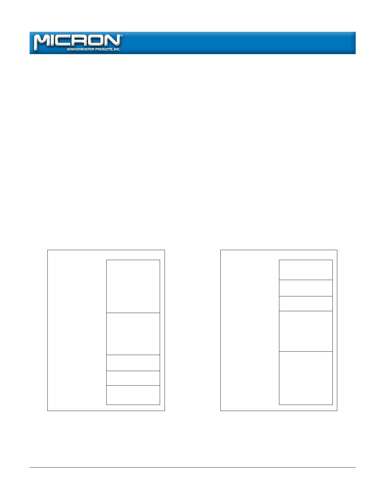
MEMORY ARCHITECTURE
The MT28F002B3 and MT28F200B3 memory array
architecture is designed to allow sections to be erased
without disturbing the rest of the array. The array is
divided into five addressable blocks that vary in size
and are independently erasable. When blocks rather
than the entire array are erased, total device endurance
is enhanced, as is system flexibility. Only the ERASE
function is block-oriented. All READ and WRITE opera-
tions are done on a random-access basis.
The boot block is protected from unintentional
ERASE or WRITE with a hardware protection circuit
which requires that a super-voltage be applied to RP# or
that the WP# pin be driven HIGH before erasure is
commenced. The boot block is intended for the core
firmware required for basic system functionality. The
remaining four blocks do not require that either of
these two conditions be met before WRITE or ERASE
operations.
BOOT BLOCK
The hardware-protected boot block provides extra
security for the most sensitive portions of the firmware.
This 16KB block may only be erased or written when the
RP# pin is at the specified boot block unlock voltage
(VHH) of 12V or when the WP# pin is VIH. During a
WRITE or ERASE of the boot block, the RP# pin must be
WORD ADDRESS BYTE ADDRESS
1FFFFH
3FFFFH
128KB Main Block
10000H
0FFFFH
20000H
1FFFFH
96KB Main Block
04000H
03FFFH
03000H
02FFFH
02000H
01FFFH
00000H
08000H
07FFFH
06000H
05FFFH
04000H
03FFFH
00000H
8KB Parameter Block
8KB Parameter Block
16KB Boot Block
WORD ADDRESS BYTE ADDRESS
1FFFFH
3FFFFH
1E000H
1DFFFH
1D000H
1CFFFH
1C000H
1BFFFH
3C000H
3BFFFH
3A000H
39FFFH
38000H
37FFFH
16KB Boot Block
8KB Parameter Block
8KB Parameter Block
96KB Main Block
10000H
0FFFFH
20000H
1FFFFH
128KB Main Block
00000H
00000H
Bottom Boot
MT28F002B3/200B3xx-xxB
Top Boot
MT28F002B3/200B3xx-xxT
Figure 1
Memory Address Maps
2Mb Smart 3 Boot Block Flash Memory
F48.p65 – Rev. 1/00
8
Micron Technology, Inc., reserves the right to change products or specifications without notice.
©2000, Micron Technology, Inc.
Share Link: 