CXA1853AQ 데이터 시트보기 (PDF) - Sony Semiconductor
부품명
상세내역
제조사
CXA1853AQ Datasheet PDF : 39 Pages
| |||
CXA1853AQ
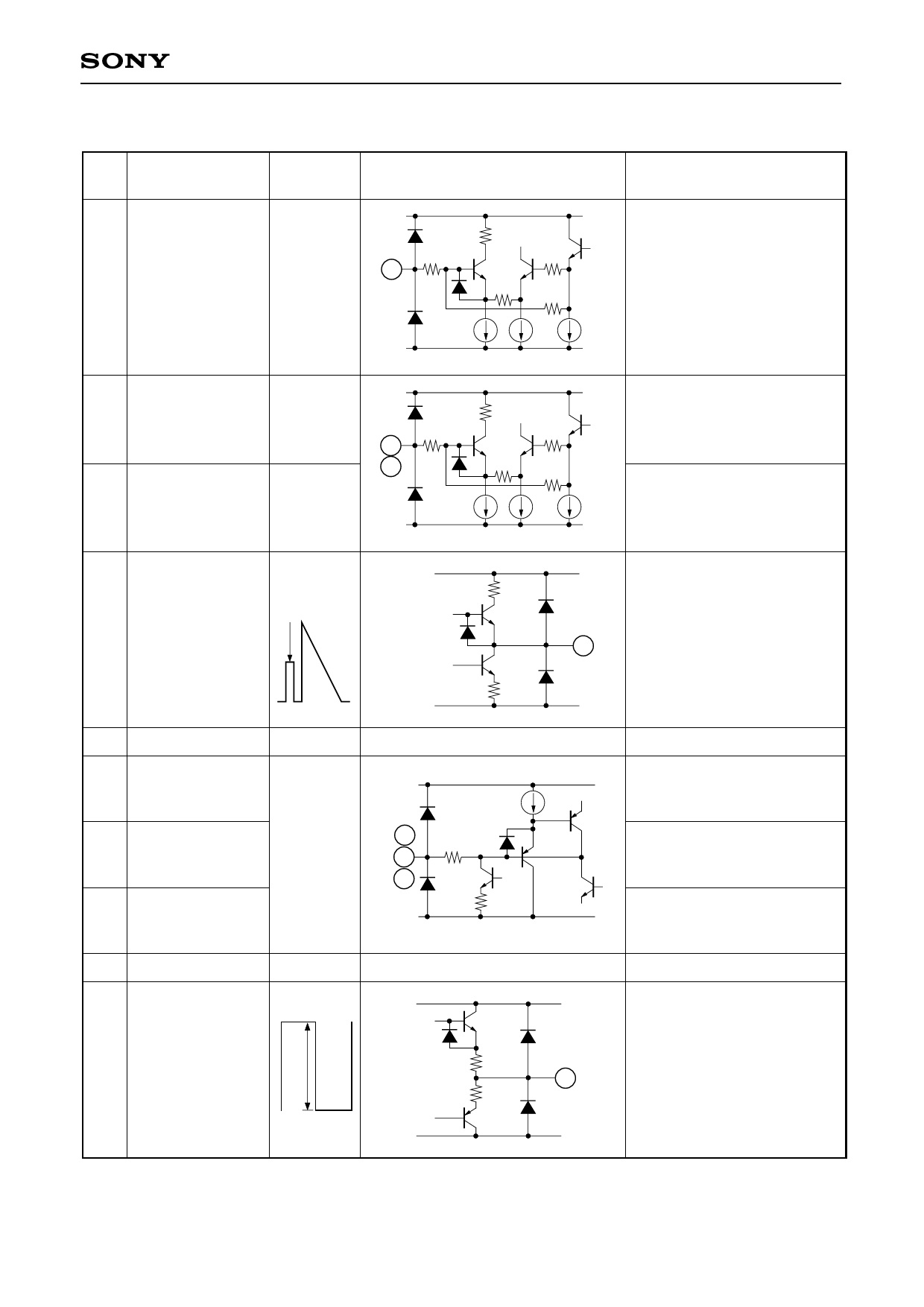
Pin Description
Pin
NO.
Symbol
1 RGB MBRT
4 R MBRT
5 B MBRT
7 GAM OUT
8 VCC1
9 RIN
10 GIN
11 BIN
12 GND
(VCC1 = 5V, VCC2 = 13V)
Pin voltage
Equivalent circuit
Description
VCC1
2k
1.6 to 5.0V∗
200
1
80k
37k
80k
GND
40µA
40µA
RGB signal common main
brightness control. Preset
internally to 3.3V.
40µA
VCC1
1.6 to 5.0V∗
5k
200
80k
4
5
74k
80k
1.6 to 5.0V∗
GND
20µA
20µA
R signal main brightness
control. Preset internally to
3.3V.
B signal main brightness
40µA control. Preset internally to
3.3V.
2V
Reference level
VCC1
100
100
GND
G signal output of which main
bright and gamma are
7
adjusted and insert the
reference signal.
5V
5V power supply.
VCC1
9
10
11
GND
50µA
200
6.2k
R signal input.
Input a 0.7Vp-p signal.Note 2)
G signal input.
Input a 0.7Vp-p signal.Note 2)
B signal input.
Input a 0.7Vp-p signal.Note 2)
0V
GND.
VCC2
13 SID OUT
9.3Vp-p
Typ.
10
13
10
GND
Note 1) ∗ in the Pin voltage indicates external applied voltage.
Note 2) Defined as the amplitude from the pedestal level to white.
–3–
SID signal output.
Share Link: 