HMS9XC7132 데이터 시트보기 (PDF) - Hynix Semiconductor
부품명
상세내역
제조사
HMS9XC7132 Datasheet PDF : 90 Pages
| |||
HMS9xC7132 / HMS9xC7134
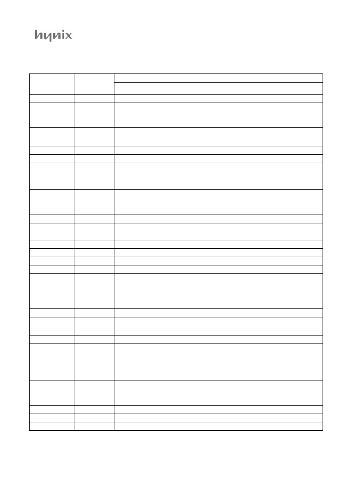
5.1 40DIP Pin Description
PIN NAME
(Alternate)
PWM0 /P2.2
DPWM0 /P2.1
DPWM0 /P2.0
RESET
VDD1
VSS1
XTAL2
XTAL1
SDA2 /P1.7
Pin
No.
In/Out
(Alter-
nate)
1
I/O
2
I/O
3
I/O
4
I
5
-
6
-
7
O
8
I
9
I/O
SCL2 /P1.6
P0.7
P0.6
P0.5
P0.4
INT0 /VPP
P0.3
P0.2
P0.1
P0.0
ACH3 /P1.5
ACH2 /P1.4
ACH0 /P1.3
ACH0 /P1.2
SDA1 /P1.1
10 I/O
11 I/O
12 I/O
13 I/O
14 I/O
15
I
16 I/O
17 I/O
18 I/O
19 I/O
20 I/O
21 I/O
22 I/O
23 I/O
24 I/O
SCL1 /P1.0
25 I/O
VSS2
26
-
VDD2
27
-
SOGin /P3.7
28 I/O
PATOUT /P3.7 29 I/O
CLAMP /PWM7 /
P3.5 /PROG
30
I/O
PWM6 /P3.4 /
INT1
31
I/O
VSYNCout /P3.3 32 I/O
HSYNCout /P3.2 33 I/O
PWM5 /P2.7
34 I/O
PWM4 /P2.6
35 I/O
PWM3 /P2.5
36 I/O
PWM2 /P2.4
37 I/O
Function
Basic
Alternate
General I/O port P2.2
General I/O port P2.1
General I/O port P2.0
Reset input
8-bit Pulse Width Modulation output0
8-bit Dynamic Pulse Width Modulation output0
8-bit Dynamic Pulse Width Modulation output1
Power supply1(+5V)
Ground1
Oscillator output pin for system clock
Oscillator input pin for system clock
General I/O port P1.7
I2C serial data I/O port
General I/O port P1.6
I2C serial clock I/O port
General I/O port P0.7; adapted for LED driver
General I/O port P1.6; adapted for LED driver
General I/O port P0.5
General I/O port P0.4
External interrupt input0; Programming supply voltage (during OTP programming)
General I/O port P0.3
General I/O port P0.2
General I/O port P0.1
General I/O port P0.0
General I/O port P1.5
General I/O port P1.4
General I/O port P1.3
General I/O port P1.2
General I/O port P1.1
General I/O port P1.0
ADC channel3 input
ADC channel2 input
ADC channel1 input
ADC channel0 input
I2C serial data I/O port for DDC interface
I2C serial clock I/O port for DDC interface
Ground2
Power supply2(+5V)
General I/O port P3.7
General I/O port P3.6
General output only port P3.5
Program pulse input(during OTP
programming)
Sync on Green input
Pattern out
Clamp out ; 8-bit Pulse Width Modulation
output7
General I/O port P3.4
8-bit Pulse Width Modulation output6; External
interrupt input1
General I/O port P3.3
General I/O port P3.2
General I/O port P2.7
General I/O port P2.6
General I/O port P2.5
General I/O port P2.4
Vertical sync output
Horizontal sync output
8-bit Pulse Width Modulation output5
8-bit Pulse Width Modulation output4
8-bit Pulse Width Modulation output3
8-bit Pulse Width Modulation output2
Table 5-1 Port Function Description(40DIP)
May.2001 ver1.1
7
Share Link: 