ST95P08B3TR 데이터 시트보기 (PDF) - STMicroelectronics
부품명
상세내역
제조사
ST95P08B3TR Datasheet PDF : 16 Pages
| |||
ST95P08
ically incremented to the next higher address after
each byte of data is shifted out. When the highest
address is reached (1FFh), the address counter
rolls over to 0h allowing the read cycle to be con-
tinued indefinitely. The read operation is terminated
by deselecting the chip. The chip can be deselected
at any time during data output. Any read attempt
during a non-volatile write cycle will be rejected and
will deselect the chip.
Byte Write Operation
Prior to any write attempt, the write enable latch
must have been set by issuing the WREN instruc-
tion. First, the device is selected (S = low) and a
serial WREN instruction byte is issued. Then, the
product is deselected by taking S high. After the
WREN instruction byte is sent, the ST95P08 will
set the write enable latch and then remain in
standby until it is deselected. Then, the write state
is entered by selecting the chip, issuing a one byte
address (A7-A0), and one byte of data. Bits 3 and
4 of the write instruction contain address bits A9
and A8 (most significant address bits). S must
remain low for the entire duration of the operation.
The product must be deselected just after the eigth
bit of data has been latched in. If not, the write
process is cancelled. As soon as the product is
deselected, the self-timed write cycle is initiated.
While the write is in progress, the status register
may be read to check BP1, BP0, WEL and WIP.
WIP is high during the self-timed write cycle. When
the cycle is close to completion, the write enable
latch is reset.
Page Write Operation
A maximum of 16 bytes of data may be written
during one non-volatile write cycle. All 16 bytes
must reside on the same page. The page write
mode is the same as the byte write mode except
that instead of deselecting after the first byte of
data, up to 15 additional bytes can be shifted in
prior to deselecting the chip. A page address begins
with address xxxx 0000 and ends with xxxx 1111.
If the address counter reaches xxxx 1111 and the
clock continues, the counter will roll over to the first
address of the page (xxxx 0000) and overwrite any
previous written data. The programming cycle will
only start if the S transition does occur at the clock
low pulse just after the eigth bit of data of a word is
received.
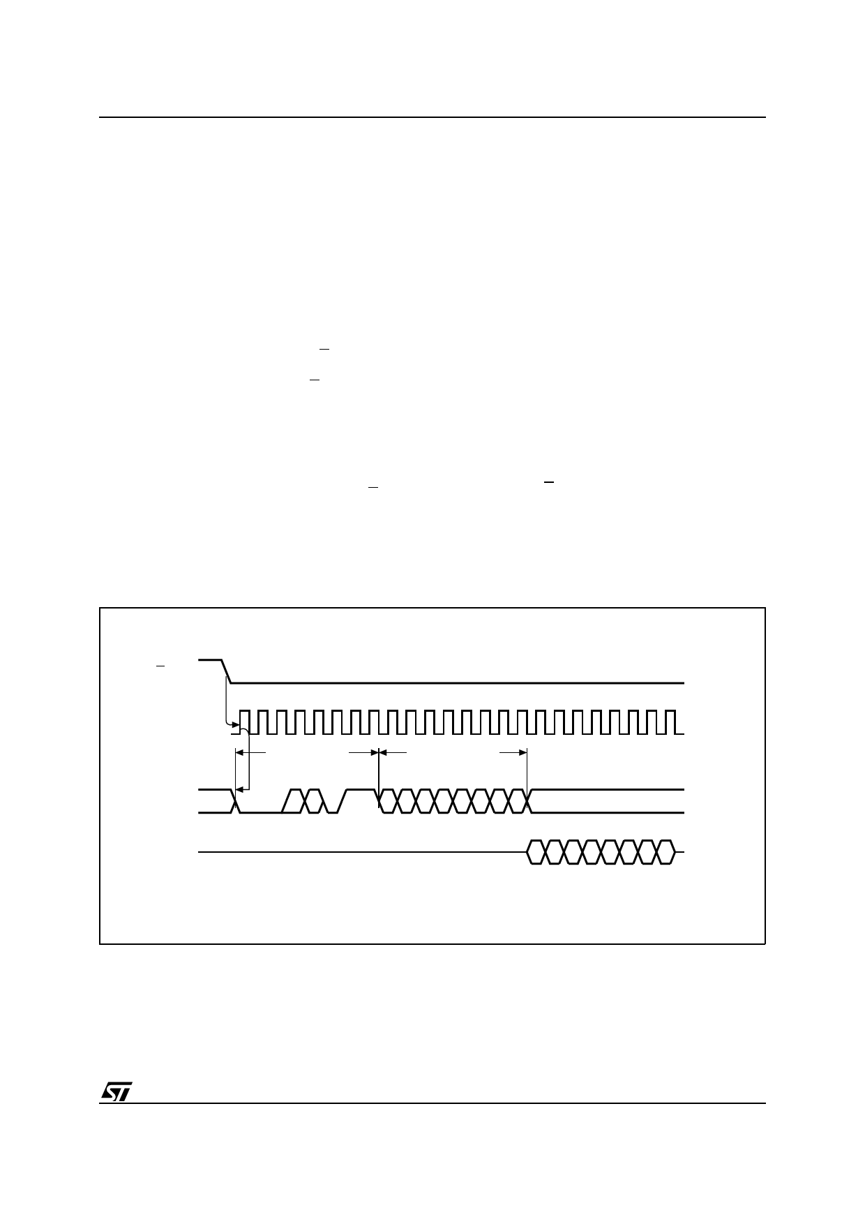
Figure 8. Read Operation Sequence
S
0 1 2 3 4 5 6 7 8 9 10 11 12 13 14 15 16 17 18 19 20 21 22 23
C
INSTRUCTION
BYTE ADDRESS
D
A9 A8
A7 A6 A5 A4 A3 A2 A1 A0
HIGH IMPEDANCE
Q
DATA OUT
76543210
AI01318
9/16
Share Link: 