CDP68HC68S1 데이터 시트보기 (PDF) - Intersil
부품명
상세내역
제조사
CDP68HC68S1 Datasheet PDF : 14 Pages
| |||
CDP68HC68S1
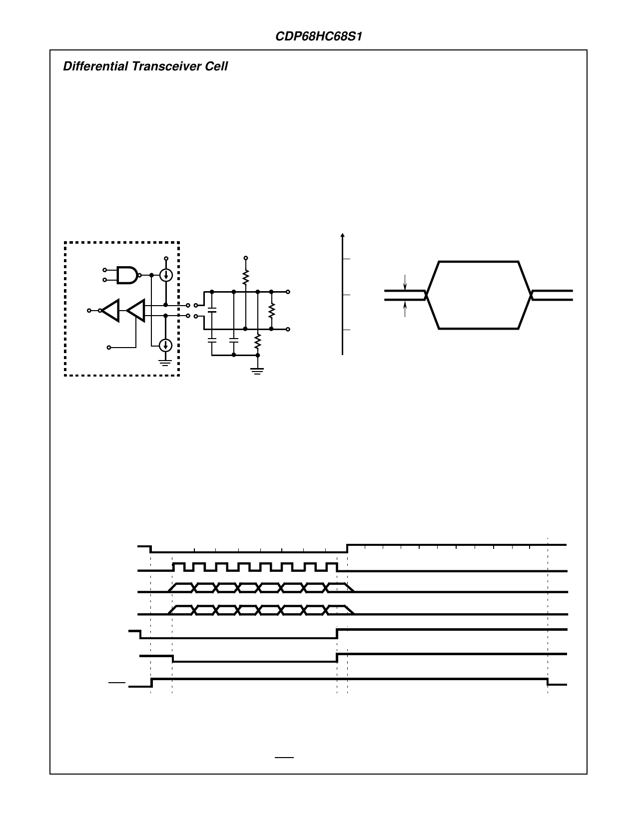
Differential Transceiver Cell
The differential transceiver is a serial interface device which
accepts digital signals and translates this information for
transmitting on the two wire differential bus.
The transmitter section (shown in Figure 4), when transmit-
ting, provides matched constant current sources to the bus
“+” and bus “-” I/O sourcing and sinking respectively. When
transmitting, a logic zero at the “transmit data” input causes
the bus “+” I/O to provide source current and the bus “-” I/O
to provide a matched sink current. A logic one at the “trans-
mit data” input causes the bus “+” and bus “-” I/Os to simulta-
neously provide a high impedance state. The bus depends
on external resistor components for bias and termination.
Recommended resistor sizes are shown in Figure 4.
SBI CHIP
TRANSMIT
---D---A----T---A----
BREAK
RECEIVE
+-
DATA
OUTOF
RANGE
VDD
IA
BUS+
BUS-
IB
VDD
13KΩ
DIFF.
BUS
CL
120Ω
DIFF.
BUS
CL CL 13KΩ
FIGURE 4. DIFFERENTIAL DRIVER/RECEIVER
A zero transmitted on the bus will appear as a large voltage
drop across the BUS+ and BUS- pins, i.e. BUS+ might typi-
cally sit at +2.8V and BUS- at +2.2V for a logic zero. For a
logic level one, the SBlC actually three-states the BUS+ and
BUS- pins and relies on external resistors to bias the bus
lines. The lines are both biased to sit at approximately 2.5V
with a small (perhaps 20mV) voltage drop across the two
lines. In this condition the BUS- line actually sits at a slightly
higher potential than the BUS+ line. See Figure 5. Thus, the
bus actually “floats” to a logic level one, but must be driven to
a logic level zero. Logic 0-bits always dominate over logic 1-
bits on the bus. If two MCU’s simultaneously transmit a zero
and a one on the bus, the zero will override the one and the
bus will merely appear to be transmitting a zero. The “mark-
ing” or idle signal on the bus is a logic one. If the bus is idle
or if a micro is sending a logic one, then a one will appear on
the bus.
In addition to the transmission of data, the differential data
transceiver accepts at its bus “+” and bus “-” I/Os, serial dif-
ferential data which is translated into the standard digital
logic levels. This reception of data also occurs while trans-
mitting, thus reflecting the data seen on the bus back into the
SBIC data register.
VDD = 5V
2.8
20mV MAX.
0.6V
2.5
BUS-
BUS+
2.2
APPROX.
VOLTAGE
LOGIC 0
LOGIC 1
LOGIC 0
Typical voltage levels seen on BUS+ and BUS-
I/O pins for logic zero and logic 1-bits. Notice
that the BUS- Pin is biased to actually sit a
higher voltage potential than the BUS+. Values
shown are for VDD = 5V
FIGURE 5.
The differential transceiver cell allows bus activity by other
devices on the bus “+” and bus “-” I/Os when power to the
cell is shut off. Therefore, this powered off condition places
the transceiver outputs, BUS “+” and BUS “-”, in a high
impedance state. When the cell is either being powered up
or down, with or without bus activity, SCR latch-up protection
is provided such that this activity is not affected.
DIFFERENTIAL
BUS
IDLE IDLE IDLE IDLE IDLE IDLE IDLE IDLE IDLE IDLE IDLE
START
BIT 0 1 2
34
5
6
STOP BIT BIT BIT BIT BIT BIT BIT BIT BIT BIT BIT
7 BIT 1 2 3 4 5 6 7 8 9 10 11
SCK
12
3
45 6
78
XMIT
REC
CONTROL (1)(3)
CONTROL (2)
MSB 6 5 4 3 2 1 LSB
MSB 6 5 4 3 2 1 LSB
(4)
IDLE
NOTES:
1. The control signal at the transmitting node.
2. The control signal at the receiving node.
3. There is a delay between the control pin being pulled low and the actual beginning of the start bit.
4. If the control pin is again puled low before the end of the stop bit, then the next start bit will begin at the end of the previous stop bit.
FIGURE 3. SCK, CONTROL, AND IDLE SIGNALS DURING THE SPI MODE OF OPERATION
6-89
Share Link: 