HT1380 데이터 시트보기 (PDF) - Holtek Semiconductor
부품명
상세내역
제조사
HT1380 Datasheet PDF : 10 Pages
| |||
HT1380/HT1381
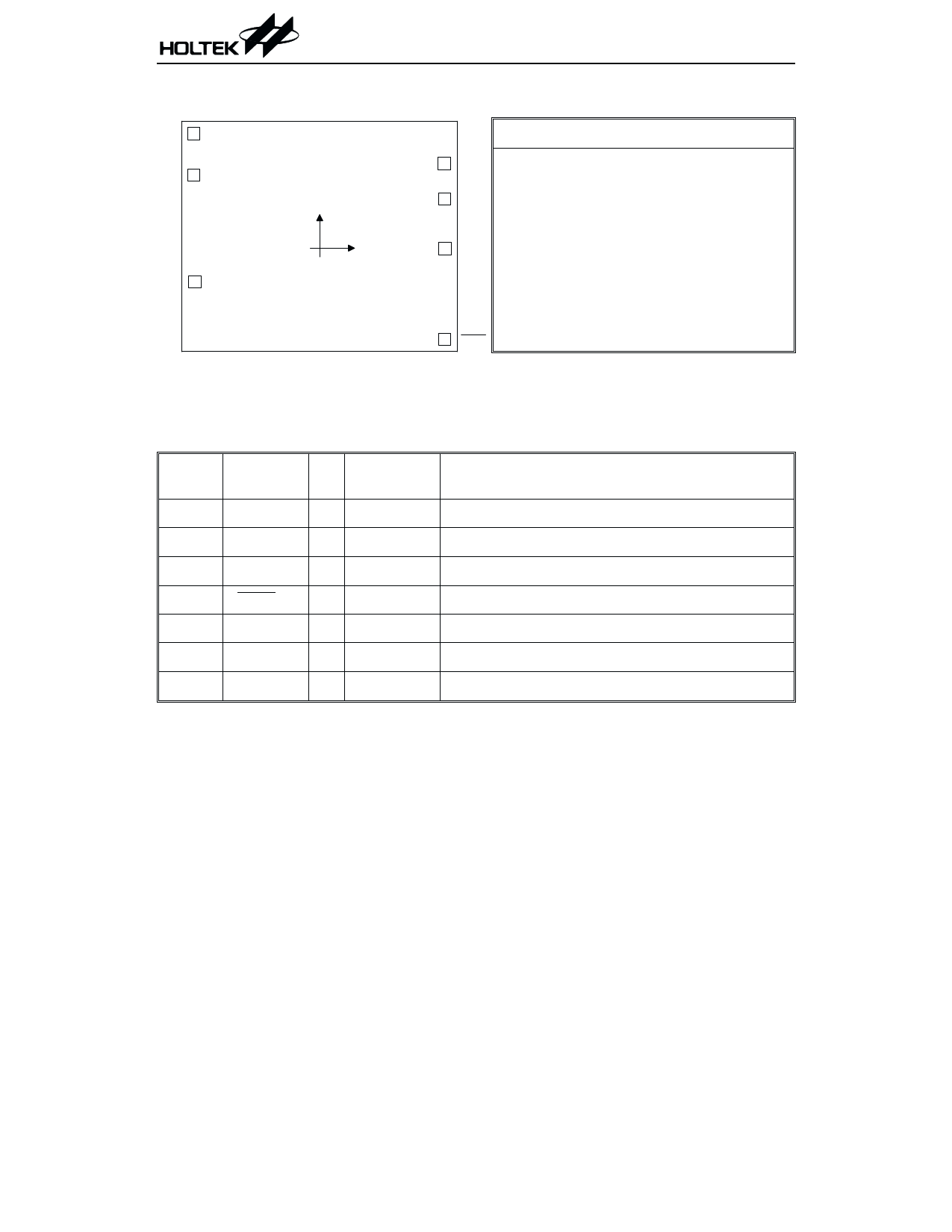
Pad Assignment
Pad Coordinates
Unit: mm
X1 1
X2 2
VSS 3
Pad No.
X
Y
7 VDD
1
-851.40
775.00
6 S C LK
2
-851.40
494.60
3
-844.40
-203.90
(0 ,0 )
5 I/O
4
845.90
-618.30
5
848.40
-4.30
6
845.90
332.60
4 REST
7
844.40
572.60
Chip size: 2010 ´ 1920 (mm)2
* The IC substrate should be connected to VSS in the PCB layout artwork.
Pad Description
Pad No. Pad Name
I/O
Internal
Connection
Description
1
X1
I
CMOS 32768Hz crystal input pad
2
X2
O
CMOS Oscillator output pad
3
VSS
¾
CMOS Negative power supply, ground
4
REST
I
CMOS Reset pin with serial transmission
5
I/O
I/O CMOS Data input/output pin with serial transmission
6
SCLK
I
CMOS Serial clock pulse pin with serial transmission
7
VDD
¾
CMOS Positive power supply
Absolute Maximum Ratings
Supply Voltage..............................-0.3V to 5.5V
Input Voltage .................VSS-0.3V to VDD+0.3V
Storage Temperature.................-50°C to 125°C
Operating Temperature ..................0°C to 70°C
Note: These are stress ratings only. Stresses exceeding the range specified under ²Absolute Maxi-
mum Ratings² may cause substantial damage to the device. Functional operation of this de-
vice at other conditions beyond those listed in the specification is not implied and prolonged
exposure to extreme conditions may affect device reliability.
2
September 18, 2000
Share Link: 