HT1380 데이터 시트보기 (PDF) - Holtek Semiconductor
부품명
상세내역
제조사
HT1380 Datasheet PDF : 10 Pages
| |||
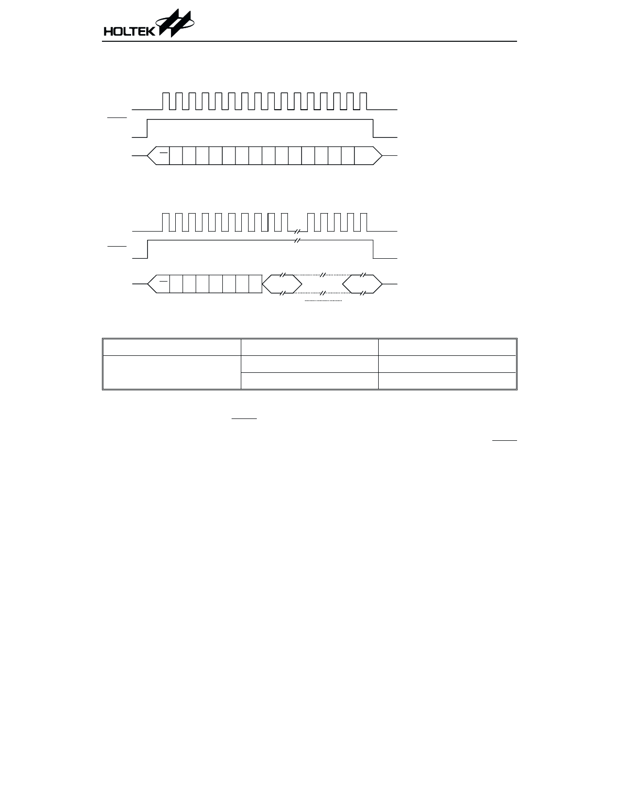
The following diagram shows the single and burst mode transfer:
S in g le b y te tr a n s fe r
S C LK
REST
I/O
0 1 2 3 4 5 6 701 2 3 4 5 67
R /W A 0 A 1 A 2 0 0 0 1
C O M M AN D BYTE
D A T A I/O
B u rs t m o d e tra n s fe r
S C LK
REST
I/O
012345670
7
R /W 1 1 1 1 1 0 1
C O M M AN D BYTE
D ATA BYTE0
0
7
D ATA BYTE7
HT1380/HT1381
The table illustrates the values suggested for capacities C1, C2
Part No.
Crystal Error
HT1380/HT1381
±10ppm
10~20ppm
Capacity Value
5pF
8pF
Operating flowchart
To initiate any transfer of data, REST is taken high and an 8-bit command byte is first loaded into the
control logic to provide the register address and command information. Following the command
word, the clock/calendar data is serially transferred to or from the corresponding register. The REST
pin must be taken low again after the transfer operation is completed. All data enter on the rising
edge of SCLK and outputs on the falling edge of SCLK. In total, 16 clock pulses are needed for a sin-
gle byte mode and 72 for burst mode. Both input and output data starts with bit 0.
In using the HT1380/HT1381, set first the WP and CH to 0 and wait for about 3 seconds, the oscilla-
tor will generate the clocks for internal use. Then, choose either single mode or burst mode to input
the data. The read or write operating flowcharts are shown on the next page.
7
September 18, 2000
Share Link: 