ICS307 데이터 시트보기 (PDF) - Integrated Circuit Systems
부품명
상세내역
제조사
ICS307 Datasheet PDF : 8 Pages
| |||
ICS307
Serially Programmable Clock Source
Setting the Device Characteristics
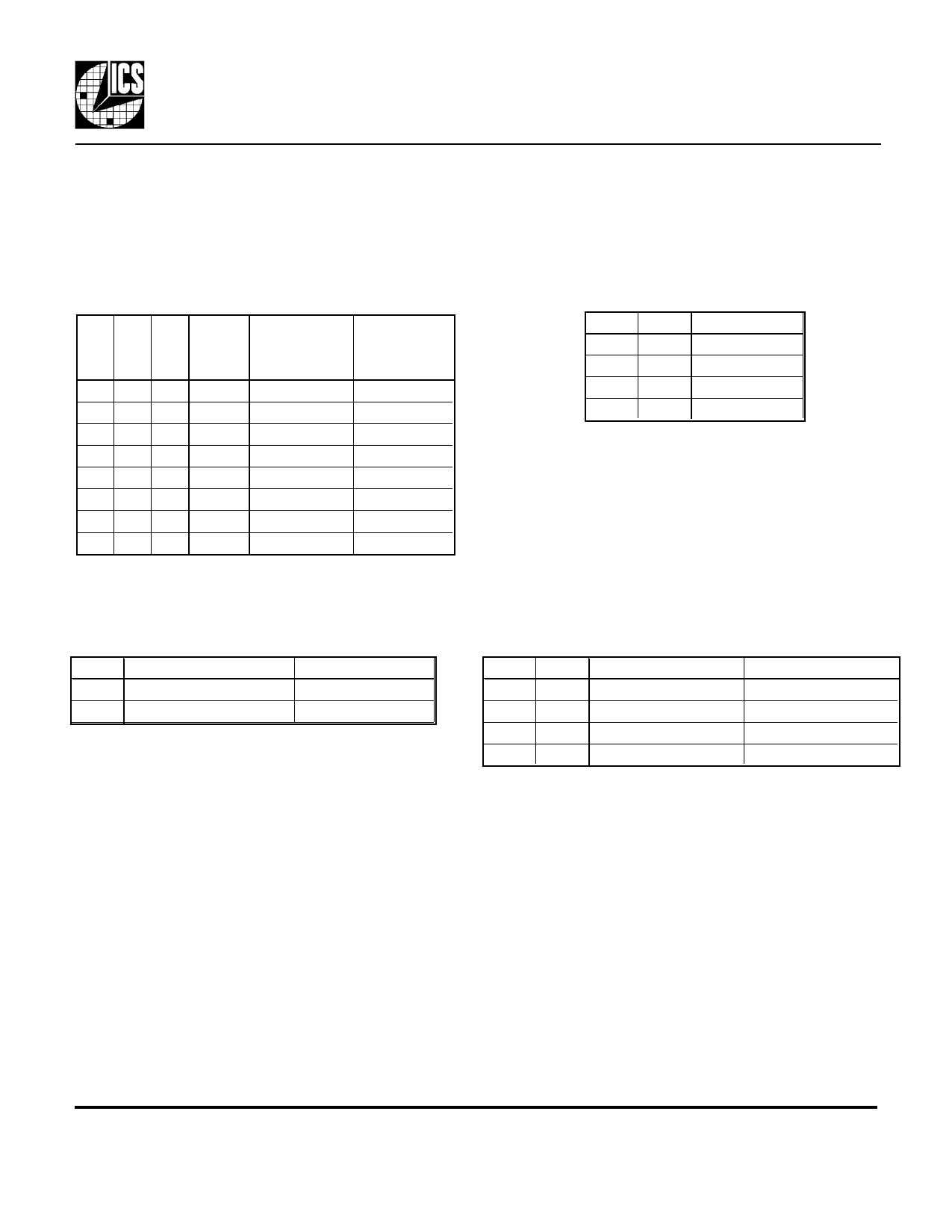
The tables below show the settings which can be configured, in addition to the VCO and Reference dividers.
Table 1. Output Divide and
Maximum Output Frequency
CLK1 Maximum Max. Freq.
S2 S1 S0 Output Frequency Industrial
Divide 5 V or 3.3 V Version
0 0 0 10
40
36
001
2
200
180
010
8
50
45
011
4
100
90
100
5
80
72
101
7
55
50
110
3
135
120
111
6
67
60
Table 2. CLK2 Output
F1 F0
0
0
0
1
1
0
1
1
CLK2
REF
REF/2
OFF (Low)
CLK1/2
0 = Connect directy to ground
1 = Connect directly to VDD
Table 3. Output Duty Cycle Configuration
TTL Duty cycle measured at Recommended VDD
0
1.4V
5V
1
VDD/2
3.3 V
Note: The TTL bit optimizes the duty cycle at
different VDD. When VDD is 5 V, set to 0
for a near-50% duty cycle with TTL levels.
When VDD is 3.3 V, set this bit to a 1, so the
50% duty cycle is achieved at VDD/2.
Table 4. Crystal Load Capacitance
C1 C0
0
0
0
1
1
0
1
1
VDD = 5 V
22.3 - 0.083 f
23.1 - 0.093 f
23.7 - 0.106 f
24.4 - 0.120 f
VDD = 3.3 V
22.1 - 0.094 f
22.9 - 0.108 f
23.5 - 0.120 f
24.2 - 0.135 f
Note: f is the crystal frequency, between 10 and
27 MHz. Effective load capacitance will be higher
for crystal frequencies lower than 10 MHz. If a
clock input is used, set C1 = 0 and C0 = 0.
MDS 307 D
4
Revision 042501
Integrated Circuit Systems, Inc. • 525 Race Street • San Jose •CA•95126•(408) 295-9800tel •www.icst.com
Share Link: 