ICS307 데이터 시트보기 (PDF) - Integrated Circuit Systems
부품명
상세내역
제조사
ICS307 Datasheet PDF : 8 Pages
| |||
ICS307
Serially Programmable Clock Source
Configuring the ICS307
The ICS307 can be programmed to set the output functions and frequencies. The three data bytes are
written to the DATA pin, in this order:
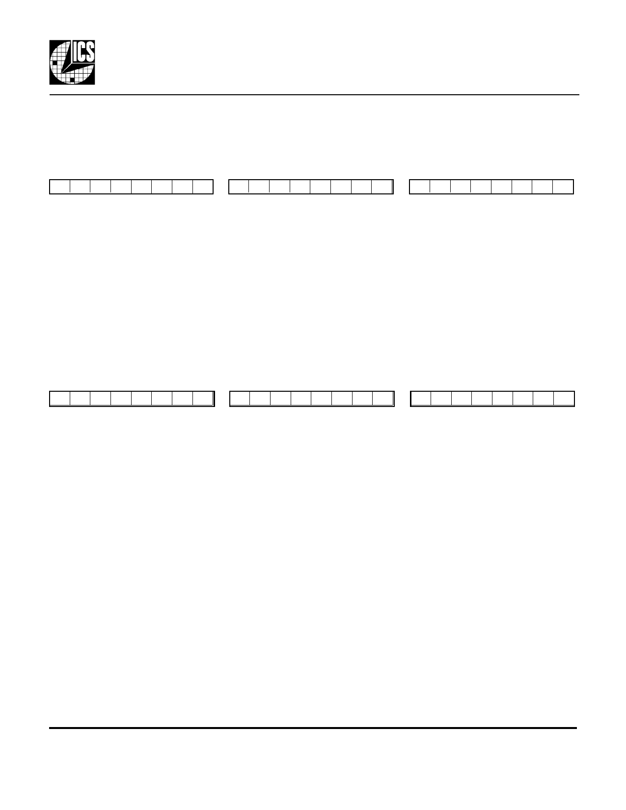
C1 C0 TTL F1 F0 S2 S1 S0 V8 V7 V6 V5 V4 V3 V2 V1
MSB
LSB MSB
LSB
C1 is loaded into the port first and R0 last.
V0 R6 R5 R4 R3 R2 R1 R0
MSB
LSB
R6:R0
V8:V0
S2:S0
F1:F0
TTL
C1:C0
Reference Divider Word (RDW)
VCO Divider Word (VDW)
Output Divider Select (OD)
Function of CLK2 Output
Duty Cycle Setting
Internal Load Capacitance for Crystal
Power up default values for ICS 307-02
00 100011
00 000100
The input frequency will come from both outputs.
00 000110
Programming Example
To generate 66.66 MHz from a 14.31818 MHz input, the RDW should be 59, the VDW should be 276,
and the Output Divide is 2. Selecting the minimum internal load capacitance, CMOS duty cycle, and CLK2
to be OFF means that the following three bytes are sent to the ICS307:
00110001
Byte 1
10001010
Byte 2
00111011
Byte 3
As shown in Figure 2, after these 24 bits are clocked into the ICS307, taking STROBE high will send this data
to the internal latch, and the CLK output will lock within 10 ms.
NOTE: If STROBE is in the high state and SCLK is pulsed, DATA is clocked directly to the internal latch
and the output conditions will change accordingly. Although this will not damage the ICS307, it is
recommended that STROBE be kept low while DATA is being clocked into the ICS307 in order to avoid
unintended changes on the output clocks.
MDS 307 D
5
Revision 042501
Integrated Circuit Systems, Inc. • 525 Race Street • San Jose •CA•95126•(408) 295-9800tel •www.icst.com
Share Link: 