NT7605H-BDT01 데이터 시트보기 (PDF) - Novatek Microelectronics
부품명
상세내역
제조사
NT7605H-BDT01 Datasheet PDF : 32 Pages
| |||
NT7605
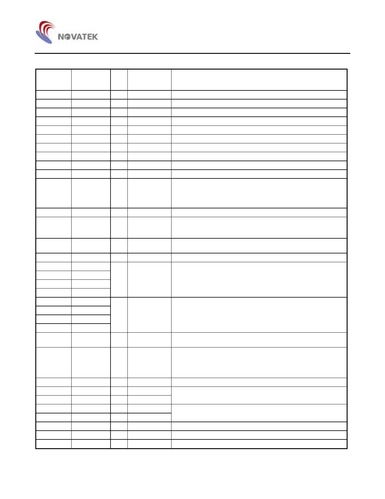
Pad Description (Total 180 pads for COG type)
Pad No.
1
2
3 - 11
12
13
14, 15
16, 17
18, 19
20, 21
22 - 26
27, 29
30 - 38
30, 40
41, 42
43, 44
45, 46
47, 48
49, 50
51, 52
53, 54
55, 56
57, 58
59, 60
61
63
64
180 - 173
65 - 72
65 - 72
180 - 173
172 - 73
73 - 172
28, 62
Designation I/O
TEST
I
TESTM
O
GND
P
OSC1
I
OSC2
O
V1
P
V2
P
V3
P
V4
P
V5
P
OPT_R0,
OPT_R1
I
VDD
P
RS
I
R/W
I
E
I
DB0
DB1
I/O
DB2
DB3
DB4
DB5
I/O
DB6
DB7
OPT_LCD I
OPT_UD
I
TESTD
O
COM1 - 8 O
COM9 - 16 O
COM1 - 8 O
COM9 - 16 O
SEG1 - 100 O
SEG1 - 100 O
GND_OUT P
External
Connection
Test pin
Test output
Power supply
Power supply
Power supply
Power supply
Power supply
Power supply
ITO Option
Power supply
MPU
MPU
MPU
Description
Test pin internally pull-down. (No connect for user)
LCD driver clock output. (No connect for user)
GND: 0V
For external clock operation, clock inputs to OSC1
Clock output
Power supply for LCD driver. VDD ≥ V1 ≥ V2 ≥ V3 ≥ V4 ≥ V5 ≥ GND
Power supply for LCD driver
Power supply for LCD driver
Power supply for LCD driver
Power supply for LCD driver
The built-in bias resister select:
OPT_R1, OPT_R0: No ITO = 1. ITO on = 0
1, 1: 2.2KΩ;
1, 0: 4KΩ;
0, 1: 6.8KΩ;
0, 0: No built-in bias resister:
VDD: +5V
Register select signal
0: Instruction register (write), Busy flag, address counter (read)
1: Data register (write, read)
Read/Write control signal
0: Write 1: Read
Read/Write start signal (Schmitt trigger input)
MPU
Lower 4 tri-state bi-directional data bus for transmitting data
between MPU and NT7605. Not used during 4-bit operation
MPU
Higher 4 tri-state bi-directional data bus for transmitting data between
MPU and NT7605. DB7 is also used as busy flag
ITO Option
ITO Option
Test output
LCD panel
LCD panel
LCD panel
LCD panel
LCD panel
LCD panel
No ITO. (Option = 1): B-Type waveform
ITO On. (Option = 0): A-Type waveform
No ITO. (Option = 1): COM1→COM8→COM9→COM16;
SEG1→SEG100
ITO On. (Option = 0): COM9→COM16→COM1→ COM8;
SEG100→SEG1
Test data output. (No connect for user)
Common signal output pins, for place on the upper glass
(OPT_UD=1)
Common signal output pins, for place on the lower glass
(OPT_UD=0)
Segment signal output pins (OPT_UD = 1)
Segment signal output pins (OPT_UD = 0)
GND output pin, use for pull-down ITO option
4
Share Link: 