CXD2719Q 데이터 시트보기 (PDF) - Sony Semiconductor
부품명
상세내역
제조사
CXD2719Q Datasheet PDF : 59 Pages
| |||
CXD2719Q
Single-Chip Dolby Pro Logic Surround Decoder
Description
The CXD2719Q is a CMOS LSI developed for
Dolby Pro Logic Surround. A SRAM for short delay
and AD/DA converters are built in, and all functions
necessary for Dolby Pro Logic Surround such as an
adaptive matrix, a passive decoder including BNR,
auto input balance, a noise sequencer and center
channel mode control are contained on a single
chip.
Features
• Dolby Pro Logic Surround decoding with a single
chip
• 2-channel 1-bit AD converter, decimation filter and
prefilter operational amplifier
• 4-channel 1-bit DA converter, oversampling filter
and post filter
• Analog switch for DSP bypass
• Analog electronic attenuator (+1.5 to –29.5dB) for
center/surround channel trim
• 24K-bit SRAM for short delay
• No separation or other variance for digital
processing
• External parts reduced by incorporating analog
circuits
Functions
• Adaptive matrix
• Center channel mode control
(Normal/Phantom/Wide)
• Dolby 3 Stereo
• Auto input balance control (ON/OFF)
• Noise sequencer
• Variable delay time (0 to 34.8ms)
• 7 kHz low-pass filter (12dB/Oct)
• Modified Dolby B-type NR
• Simple SFC function
• SFC mode
• DSP bypass mode (L, R-channel through)
Structure
Silicon gate CMOS
Applications
Equipment having Dolby Pro Logic Surround
function such as AV amplifiers, receivers and
compact music systems
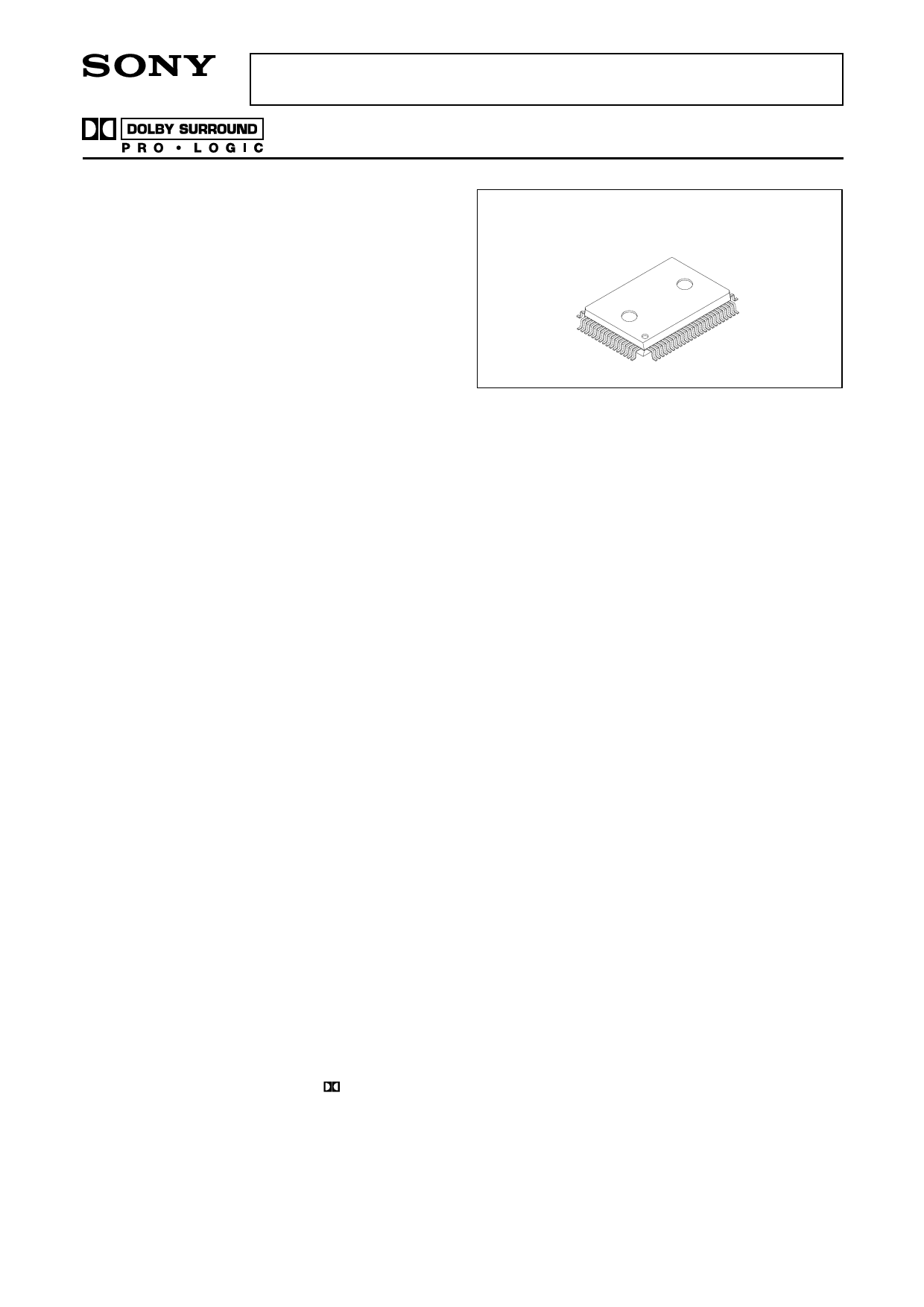
80 pin QFP (Plastic)
Absolute Maximum Ratings (Ta = 25°C, VSS = 0V)
• Supply voltage VDD VSS – 0.5 to +7.0
V
• Input voltage
VI VSS – 0.5 to VDD + 0.5 V
• Output voltage VO VSS – 0.5 to VDD + 0.5 V
• Operating temperature
Topr
–20 to +70
°C
• Storage temperature
Tstg –55 to +150
°C
Recommended Operating Conditions
• Supply voltage VDD
Analog system
4.75 to 5.25 (5.0 typ.) V
Digital system
4.50 to 5.25 (5.0 typ.) V
• Operating temperature
Ta
–20 to +70
°C
Input/Output Capacitance
• Input capacitance CIN
9 (max.)
pF
• Output capacitance COUT
11 (max.)
pF
• Input/output capacitance
CI/O
11 (max.)
pF
∗ Measurement conditions: VDD = VI = 0V, F = 1MHz
Maximum Current Consumption
(Ta = 25°C, VDD = 5.25V)
• Digital/analog block total: 166.7mA
Dolby level
• During analog input: 200 to 300mVrms
• During digital input: –20dBFS
Analog characteristics
Pro Logic ON: Dolby level = 300mVrms
Prefilter gain = –3.52dB
• S/N: L, Rch = 80dB, C, Sch = 72dB
• THD + N: L, Rch = 0.015%, C, Sch = 0.03%
∗ All values for typ.
This device is available only to parties obtaining the license from Dolby Laboratories Licensing Corporation.
"Dolby", the double-D symbol and "Pro Logic" are trademarks of Dolby Laboratories Licensing Corporation.
Sony reserves the right to change products and specifications without prior notice. This information does not convey any license by
any implication or otherwise under any patents or other right. Application circuits shown, if any, are typical examples illustrating the
operation of the devices. Sony cannot assume responsibility for any problems arising out of the use of these circuits.
–1–
E98944A13-PS
Share Link: 