UPD16732AN-XXX 데이터 시트보기 (PDF) - NEC => Renesas Technology
부품명
상세내역
제조사
UPD16732AN-XXX
NEC => Renesas Technology

UPD16732AN-XXX Datasheet PDF : 24 Pages
| |||
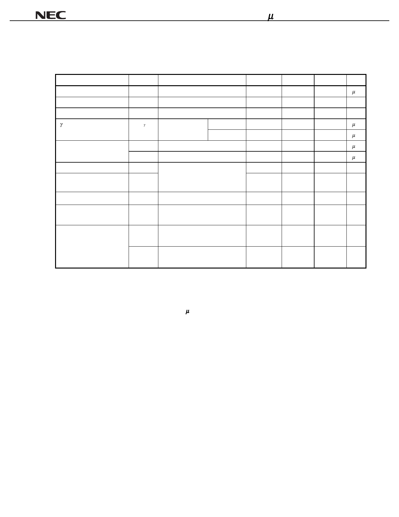
µ PD16732A, 16732B
Electrical Characteristics (TA = –10 to +75 °C, VDD1 = 2.3 V to 3.6 V, VDD2 = 8.5 V ± 0.5 V, VSS1 = VSS2 = 0 V,
Unless otherwise specified, the input level is defined to be LPC = H or Open,
Bcont = Open)
Parameter
Input Leak Current
High-Level Output Voltage
Low-Level Output Voltage
γ -Corrected Supply Current
Driver Output Current
Output Voltage Deviation
Output swing difference
deviation
Output Voltage Range
Logic Part Dynamic Current
Consumption
Driver Part Dynamic
Current Consumption
Symbol
IIL
VOH
VOL
Iγ
IVOH
IVOL
∆VO
∆VP–P
VO
IDD1
IDD21
IDD22
Condition
STHR (STHL), IOH = 0 mA
STHR (STHL), IOL = 0 mA
V0 to V4 =
V0 pin, V5 pin
V5 to V9 = 4.0 V
V4 pin, V9 pin
VX = 7.0 V, VOUT = 6.5 VNote
VX = 1.0 V, VOUT = 1.5 VNote
VDD1 = 3.3 V, VDD2 = 8.5 V,
VOUT = 2.0 V, 4.25 V, 6.5 V
All Input data
VDD1, with no load
VDD2 = 8.5 V ± 0.5 V, with no load
LPC = H, Bcont = Open
VDD2 = 8.5 V ± 0.5 V, with no load
LPC = L, Bcont = Open
MIN.
VDD1 − 0.1
126
–504
30
0.1
TYP.
252
–252
±7
±2
MAX.
Unit
±1.0
µA
V
0.1
V
504
µA
–126
µA
–30
µA
µA
±20
mV
±15
mV
VDD2 – 0.1
V
3.0
6.0
mA
3.0
6.0
mA
2.0
4.0
mA
Notes1. VX refers to the output voltage of analog output pins S1 to S384.
2. VOUT refers to the voltage applied to analog output pins S1 to S384.
Cautions 1. The STB cycle is defined to be 20 µs at fCLK = 40 MHz.
2. The TYP. values refer to an all black or all white input pattern. The MAX. value refers to the
measured values in the dot checkerboard input pattern.
3. Refers to the current consumption per driver when cascades are connected under the
assumption of XGA single-sided mounting (8 units).
Data Sheet S13972EJ3V0DS00
15
Share Link: