ILC6360 데이터 시트보기 (PDF) - Impala Linear Corporation
부품명
상세내역
제조사
ILC6360 Datasheet PDF : 14 Pages
| |||
Step-Up/Step-Down DC-DC Converter for 1-Cell Lithium-Ion Batteries
Layout And Grounding Considerations
High frequency switching and large peak currents means
PCB design for DC-DC converters requires careful consid-
eration. A general rule is to place the DC-DC converter cir-
cuitry well away from any sensitive RF or analog compo-
nents. The layout of the DC-DC converters and its external
components are also based on some simple rules to mini-
mize EMI and output voltage ripple.
Layout
1. Place all power components, ILC6360, inductor, input
capacitor and output capacitor as close together as possible.
2. Keep the output capacitor as close to the ILC6360 as
possible with very short traces to the VOUT and GND pins.
Typically it should be within 0.25 inches or 6mm.
3. Keep the traces for the power components wide, typically >
50mil or 1.25mm.
4. Place the external networks for LBI and VFB close to the
ILC6360, but away from the power components as far
as possible.
Grounding
1. Use a star grounding system with separate traces for the
power ground and the low power signals such as LBI/SD
and VFB. The star should radiate from where the power
supply enters the PCB.
2. On multilayer boards use component side copper for
grounding around the ILC6360 and connect back to a
quiet ground plane using vias.
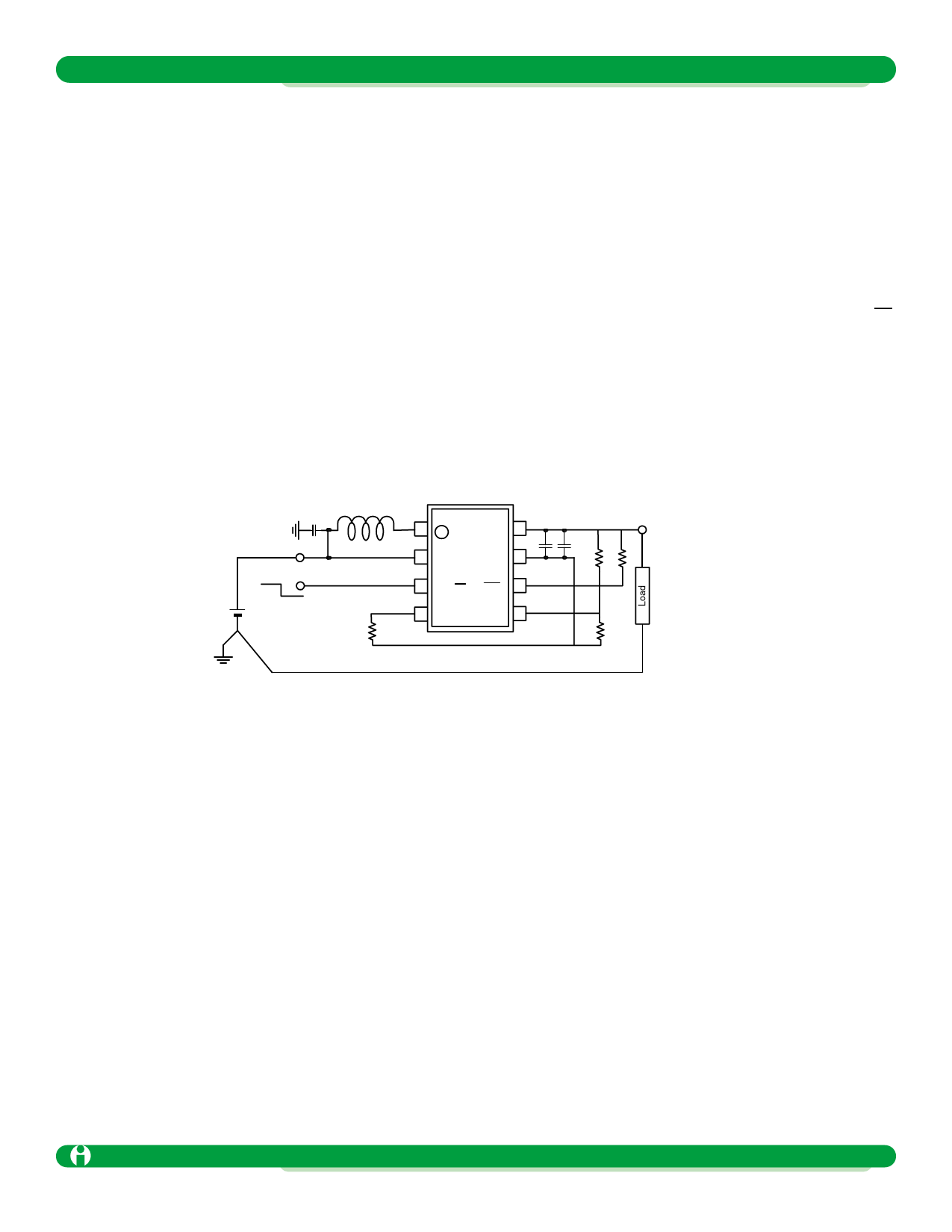
CIN
100µF
VIN
L1
15µH
ON/OFF
R4
ILC6360CIR-ADJ
COUT
10µF 100µF
1
LX
VOUT 8 + +
2 VIN
GND 7
R1
3 LBI/SD LBO 6
4 SYNC
VFB 5
R2
Local "Quiet" Ground
Power Ground
VOUT
R3
Impala Linear Corporation
ILC6360 1.1
(408) 574-3939 www.impalalinear.com
Jan 1999 9
Share Link: 