CXA2016S 데이터 시트보기 (PDF) - Sony Semiconductor
부품명
상세내역
제조사
CXA2016S Datasheet PDF : 12 Pages
| |||
CXA2016S
Pin
Pin
Symbol
No
voltage
13 CLP OUT —
14 CLP OUT —
15 CLP SEL —
16
PH
—
17
PV
18
HD
—
19 VSS OUT
—
20 VSS IN
—
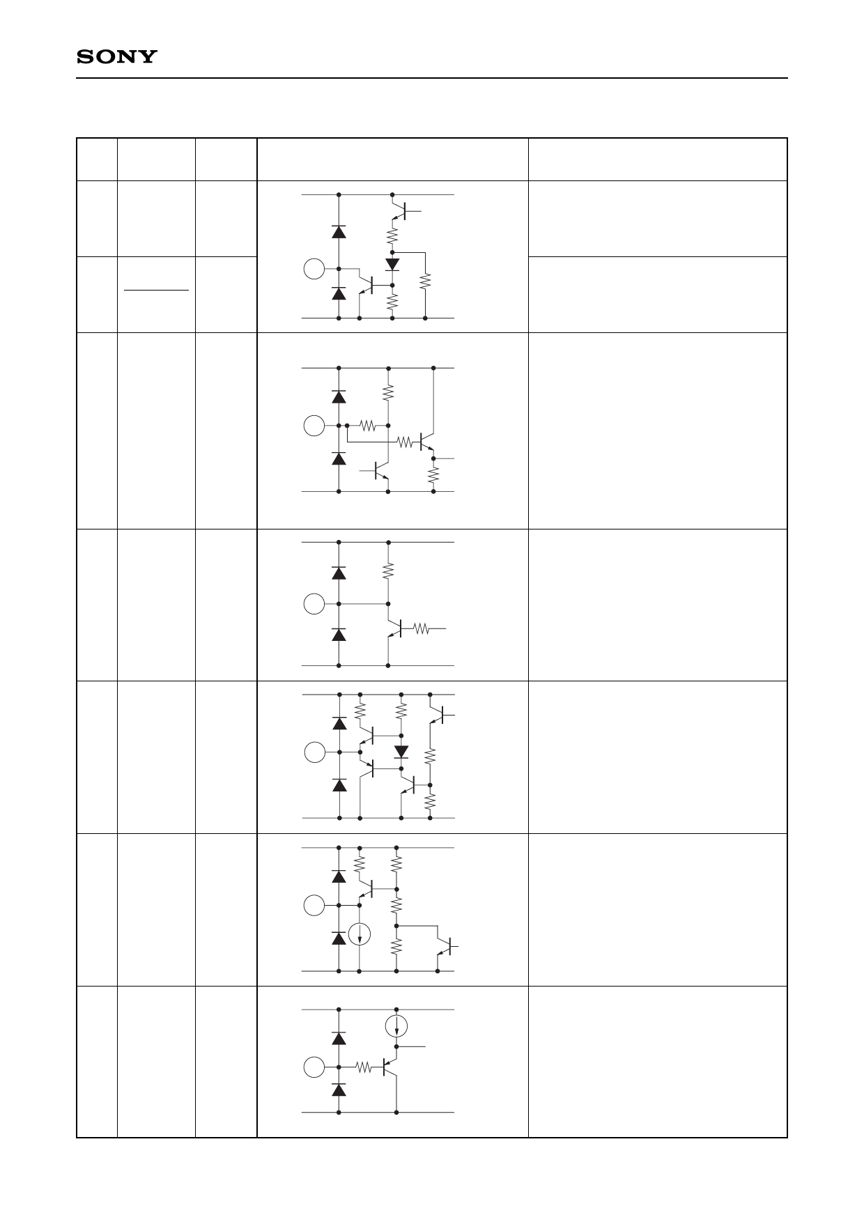
Equivalent circuit
VCC
500
13
40k
7k
GND
VCC
30k
20k
15
1k
43k
GND
VCC
20k
16
20k
333 6k
GND
VCC
18
6k
6k
GND
VCC
200 5k
19
2.5k
17.5k
GND
VCC
20
1k
GND
—4—
Description
Clamp pulse output; Open collector-
type pin at positive polarity.
Clamp pulse output; Open collector-
type pin at negative polarity.
Selects output position of a clamp
pulse. Input at TTL level.
When Low level is selected, a clamp
pulse is output at a back porch
interval.
When High level is selected, clamp
pulse is output at a sync interval.
See the Description of Operation for
Input/Output Matrix.
Output polarity information of
horizontal and vertical sync signals.
See the Description of Operation for
Input/Output Matrix.
HD (H. Drive Pulse) output; Push-pull
type pin at positive polarity.
Composite sync or sync signal
separated from video sync is output.
Output is at positive polarity.
Input for V. sync separator
comparator. Integrates the output at
Pin 19 and inputs it.
Share Link: 