L6234(2003) 데이터 시트보기 (PDF) - STMicroelectronics
부품명
상세내역
제조사
L6234 Datasheet PDF : 11 Pages
| |||
L6234
ABSOLUTE MAXIMUM RATINGS
Symbol
VS
VIN,VEN
Ipeak
VSENSE
Vb
VOD
fC
VREF
Ptot
Ptot
Tstg, Tj
Power Supply Voltage
Parameter
Input Enable Voltage
Pulsed Output Current (note 1)
Sensing Voltage (DC Voltage)
Bootstrap Peak Voltage
Differential Output Voltage (between any of the 3 OUT pins)
Commutation Frequency
Reference Voltage
Total Power Dissipation
Total Power Dissipation
L6234PD Tamb = 70°C
L6234 Tamb = 70°C
Storage and Junction Temperature Range
Note 1: Pulse width limited only by junction temperature and the transient thermal impedance
(*) Mounted on board with minimized copper area
RECOMMENDED OPERATING CONDITIONS
Value
52
– 0.3 to 7
5
-1 to 4
62
60
50
12
2.3
1.6 (*)
-40 to 150
Unit
V
V
A
V
V
V
KHz
V
W
W
°C
Symbol
VS
VOD
Supply Voltage
Parameter
Peak to Peak Differential Voltage (between any of the 3 OUT
pins)
Value
Unit
7 to 42
V
52
V
Iout
DC Output Current Power SO20 (Tamb = 25°C)
4
A
DC Output Current Power DIP (Tamb = 25°C) with infinite heatsink
2.8
A
VSENSE Sensing Voltage (pulsed tw < 300nsec)
-4 to 4
V
Sensing Voltage (DC)
-1 to 1
V
Tj
Junction Temperature Range
-40 to 125
°C
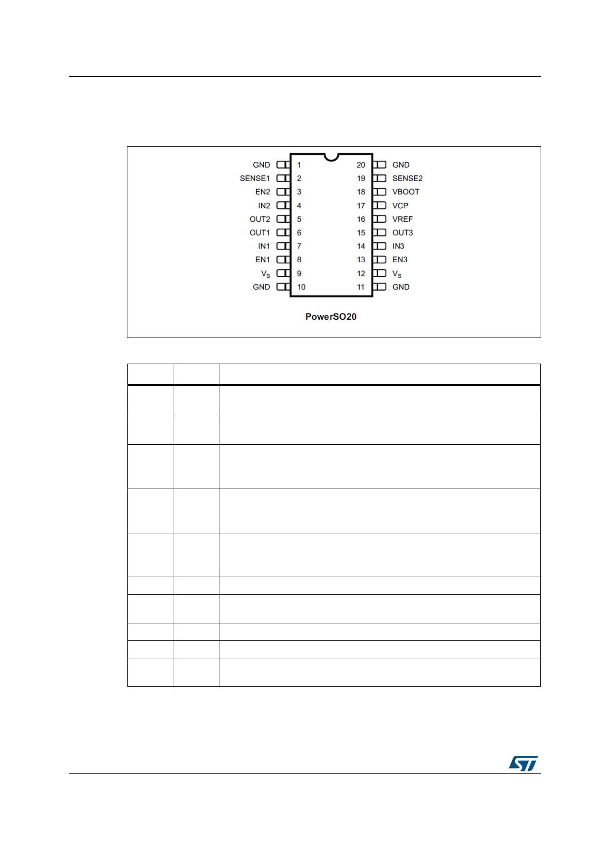
PIN FUNCTIONS
Powerdip
1
20
10
PowerSO20
6
5
15
Name
OUT 1
OUT 2
OUT 3
Output of the channels 1/2/3.
Function
2
7
IN 1 Logic input of channels 1/2/3. A logic HIGH level (when the corresponding
19
4
IN 2 EN pin is HIGH) switches ON the upper DMOS Power Transistor, while a
9
14
IN 3 logic LOW switches ON the corresponding low side DMOS Power.
3
8
EN 1 Enable of the channels 1/2/3. A logic LOW level on this pin switches off both
18
3
EN 2 power DMOS of the related channel.
8
13
EN 3
4,7
9, 12
Vs
Power Supply Voltage.
14
19
SENSE2 A resistance Rsense connected to this pin provides feedback for motor
current control for the bridge 3.
17
2
SENSE1 A resistance Rsense connected to this pin provides feedback for motor
current control for the bridges 1 and 2.
11
16
Vref Internal Voltage Reference. A capacitor connected from this pin to GND
increases the stability of the Power DMOS drive circuit.
12
13
5,6
15,16
17
18
1,10
11,20
Vcp
VBOOT
GND
Bootstrap Oscillator. Oscillator output for the external charge pump.
Overvoltage input to drive the upper DMOS
Common Ground Terminal. In Powerdip and SO packages these pins are
used to dissipate the heat forward the PCB.
4/10
Share Link: 