EL2360CS 데이터 시트보기 (PDF) - Elantec -> Intersil
부품명
상세내역
제조사
EL2360CS Datasheet PDF : 16 Pages
| |||
EL2360C
Triple 130 MHz Current Feedback Amplifier
Absolute Maximum Ratings (TA e 25 C)
Voltage between VSa and VSb
Common-Mode Input Voltage
Differential Input Voltage
a33V
VSb to VSa
g6V
Current into aIN or bIN
g10 mA
Internal Power Dissipation
See Curves
Output Current (continuous)
Operating Ambient Temperature Range
Operating Junction Temperature
Storage Temperature Range
g50 mA
b40 C to a85 C
150 C
b65 C to a150 C
Important Note
All parameters having Min Max specifications are guaranteed The Test Level column indicates the specific device testing actually
performed during production and Quality inspection Elantec performs most electrical tests using modern high-speed automatic test
equipment specifically the LTX77 Series system Unless otherwise noted all tests are pulsed tests therefore TJeTCeTA
Test Level
I
II
III
IV
V
Test Procedure
100% production tested and QA sample tested per QA test plan QCX0002
100% production tested at TA e 25 C and QA sample tested at TA e 25 C
TMAX and TMIN per QA test plan QCX0002
QA sample tested per QA test plan QCX0002
Parameter is guaranteed (but not tested) by Design and Characterization Data
Parameter is typical value at TA e 25 C for information purposes only
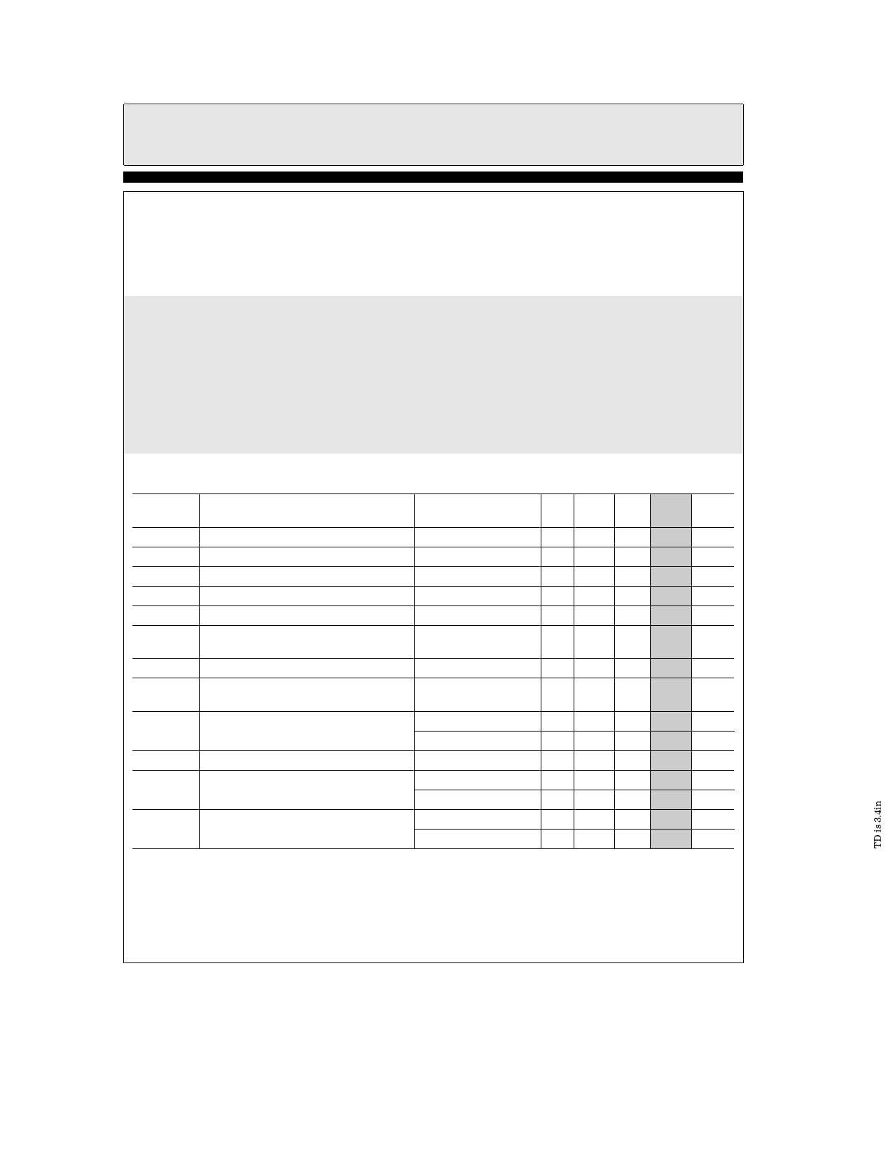
DC Electrical Characteristics VS e g15V RLe150X TAe25 C unless otherwise specified
Parameter
Description
Conditions
Min Typ Max Test Units
Level
VOS
TCVOS
aIIN
bIIN
CMRR
bICMR
Input Offset Voltage
VS e g5V g15V
Average Input Offset Voltage Drift (Note 1)
aInput Current
bInput Current
Common Mode Rejection Ratio (Note 2)
bInput Current Common
Mode Rejection (Note 2)
VS e g5V g15V
VS e g5V g15V
VS e g5V g15V
VS e g5V g15V
2
10
10
05
3
5
25
50 55
02
5
I
mV
V mV C
I
mA
I
mA
I
dB
I mA V
PSRR
Power Supply Rejection Ratio (Note 3)
75
95
I
dB
bIPSR
bInput Current Power
Supply Rejection (Note 3)
02
5
I mA V
ROL
aRIN
aCIN
Transimpedance (Note 4)
a Input Resistance
a Input Capacitance
VS e g15V RL e 400X 500
VS e g15V RL e 150X 500
15
PDIP package
SOIC package
2000
1800
3
15
1
I
kX
I
kX
I
MX
V
pF
V
pF
CMIR
Common Mode Input Range
VS e g15V
VS e g5V
Note 1 Measured from TMIN to TMAX
Note 2 VCM e g10V for VS e g15V VCM e g3V for VS e g5V
Note 3 The supplies are moved from g2 5V to g15V
Note 4 VOUT e g7V for VS e g15V VOUT e g2V for VS e g5V
g13 5
g3 5
V
V
V
V
2
Share Link: 