EL4332C 데이터 시트보기 (PDF) - Elantec -> Intersil
부품명
상세내역
제조사
EL4332C Datasheet PDF : 17 Pages
| |||
EL4332C
Triple 2:1 300 MHz Mux-Amp AV =2
Grounds
It will be noticed that each mux-amp channel has its own
separate ground pin. These ground pins have been kept
separate to keep the channel separation inside the chip as
large as possible. The feedback resistors use these
ground pins as their reference. The resistors total 400Ω,
so there is a significant signal current flowing from these
pins to ground.
The ground pins should all be connected together, to a
ground plane underneath the chip. 1 oz. copper for the
ground plane is highly recommended.
Further notes and recommended practices for high speed
printed circuit board layout can be found in the tutorials
in the Elantec databooks.
Supplies
Supply bypassing should be as physically near the power
pins as possible. Chip capacitors should be used to mini-
mize lead inductance. Note that larger values of
capacitor tend to have larger internal inductances. So
when designing for 3 transmission lines or similar mod-
erate loads, a 0.1 µF ceramic capacitor right next to the
power pin in parallel with a 22 µF tantalum capacitor
placed as close to the 0.1 µF is recommended. For lighter
loadings, or if not all the channels are being used, a sin-
gle 4.7 µF capacitor has been found quite adequate.
Note that component video signals do tend to have a
high level of signal correlation. This is especially true if
the video signal has been derived from 3 synchronously
clocked DACs. This corresponds to all three channels
drawing large slew currents simultaneously from the
supplies. Thus, proper bypassing is critical.
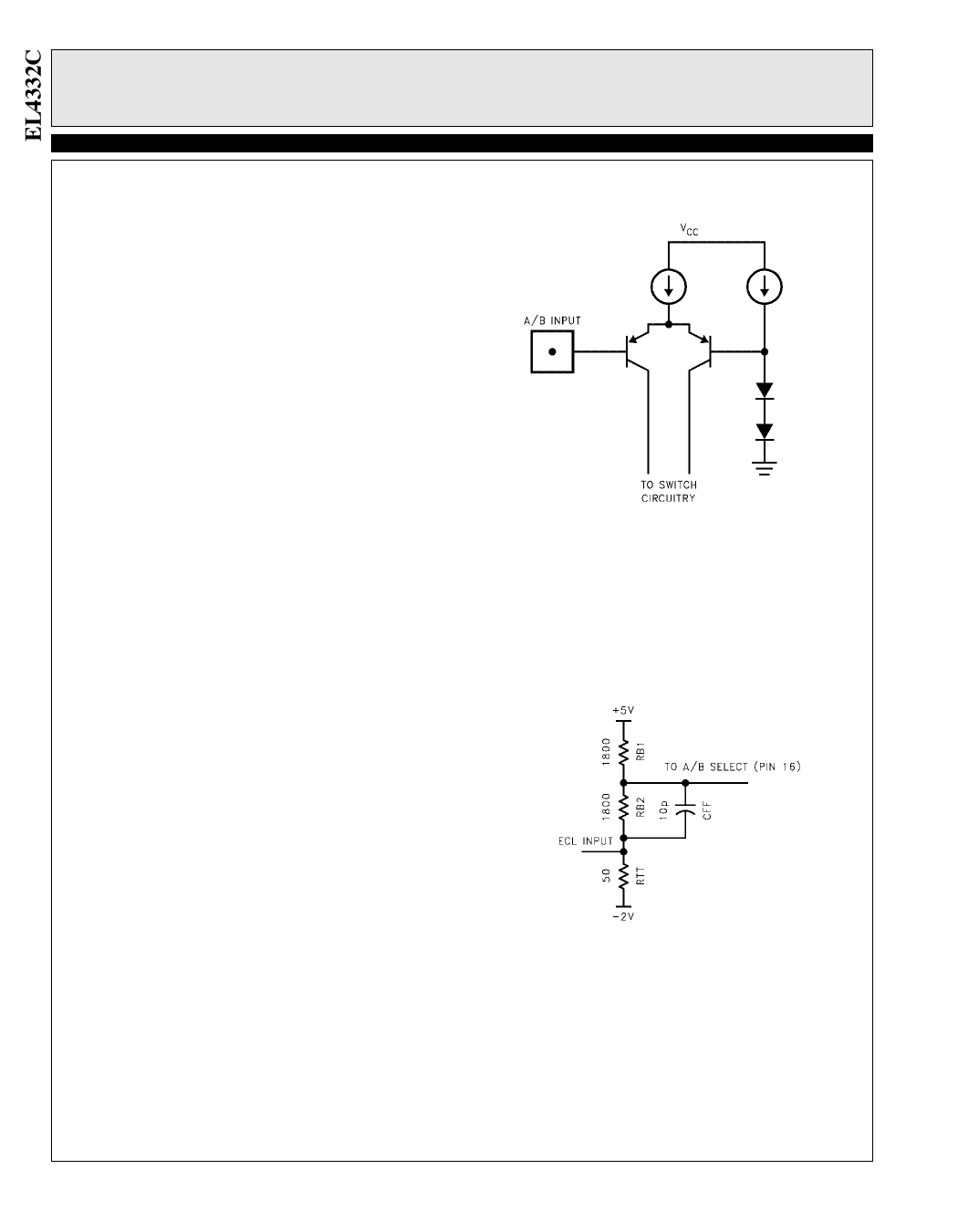
current, typically < 30 µA, for a logic “low”. If left to
float, it will be a logic “high”.
Figure 2. Simplified Logic Input Stage
The input PNP transistors have sufficient gain that a
simple level shift circuit (see Figure 3) can be used to
provide a simple interface with Emitter Coupled Logic.
Typically, 200 mV is enough to switch from a solid
logic “low” to a “high.”
Logic Inputs
The A/B select, logic input, is internally referenced to
ground. It is set at 2 diode drops above ground, to give a
threshold of about 1.4V (see Figure 2). The PNP input
transistor requires that the driving gate be able to sink
Figure 3. Adapting the Select Pin
for ECL Logic Levels
The capacitor Cff is only in the network to prevent the
A/B pin’s capacitance from slowing the control signal.
The network shown level shifts the ECL levels, -0.7V to
-1.5V to +1.6V and +1.1V respectively. The terminating
resistor, Rtt, is required since the open emitter of the
ECL gate can not sink current. If a -2V rail is not being
10
Share Link: 