MAX4565 데이터 시트보기 (PDF) - Maxim Integrated
부품명
상세내역
제조사
MAX4565 Datasheet PDF : 16 Pages
| |||
Quad/Dual, Low-Voltage,
Bidirectional RF/Video Switches
______________________________________________________________Pin Description
MAX4565
1, 10, 11,
20
3, 6, 8, 13,
15, 18
16
PIN
MAX4566
1, 16
3, 7, 10, 14
12
MAX4567
1, 9
4, 6, 12, 14
7, 15
NAME
IN_
GND_
V+
5
5
3, 11
V-
4, 7, 14, 17
—
2, 9, 12, 19
4, 13
6, 11
2, 8, 9, 15
2, 16
8, 10
5, 13
NO_
NC_
COM_
FUNCTION*
Digital Control Input
RF and Logic Ground. Grounds are not internally connected to each other,
and should all be connected to a ground plane (see Grounding section).
Positive Supply-Voltage Input (analog and digital)
Negative Supply-Voltage Input. Connect to ground plane for single-supply
operation.
Analog Switch Normally Open** Terminals
Analog Switch Normally Closed** Terminals
Analog Switch Common** Terminals
* All pins have ESD diodes to V- and V+.
** NO_ (or NC_) and COM_ pins are identical and interchangeable. Either may be considered as an input or output; signals pass
equally well in either direction.
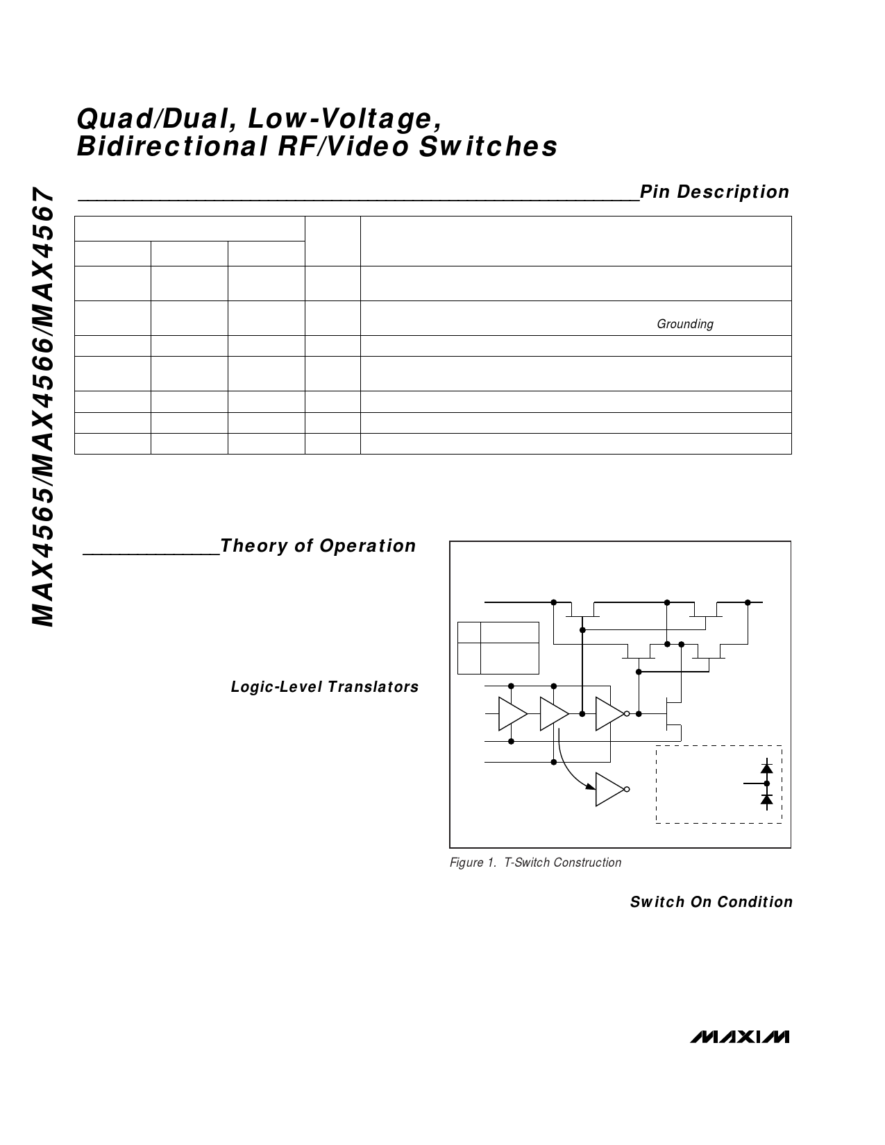
_______________Theory of Operation
The MAX4565/MAX4566/MAX4567 are high-frequency
“T” switches. Each “T” switch consists of two series
CMOS switches, with a third N-channel switch at the
junction that shunts capacitively-coupled signals to
ground when the series switches are off. This produces
superior high-frequency signal isolation when the
switch is turned off.
Logic-Level Translators
The MAX4565/MAX4566/MAX4567 are constructed as
high-frequency “T” switches, as shown in Figure 1. The
logic-level input, IN_, is translated by amplifier A1 into a
V+ to V- logic signal that drives amplifier A2. (Amplifier
A2 is an inverter for normally closed switches.)
Amplifier A2 drives the gates of N-channel MOSFETs
N1 and N2 from V+ to V-, turning them fully on or off.
The same signal drives inverter A3 (which drives the
P-channel MOSFETs P1 and P2) from V+ to V-, turning
them fully on or off, and drives the N-channel MOSFET
N3 off and on.
The logic-level threshold is determined by V+ and
GND_. The voltage on GND_ is usually at ground
potential, but it may be set to any voltage between
(V+ - 2V) and V-. When the voltage between V+ and
GND_ is less than 2V, the level translators become very
slow and unreliable. Since individual switches in each
package have individual GND_ pins, they may be set to
different voltages. Normally, however, they should all
be connected to the ground plane.
NORMALLY OPEN SWITCH CONSTRUCTION
COM_
IN_ COM_ - NO_
0
OFF
1
ON
N1
D
S
N2
D
S
P1
S
D
P2
S
D
V+
IN_
GND_
V-
A1
A2
D
A3
N3
S
A2
ESD DIODES
(NC)
ON GND_, IN_,
COM_, NO_, AND NC_
NO_
V+
V-
Figure 1. T-Switch Construction
Switch On Condition
When the switch is on, MOSFETs N1, N2, P1, and P2
are on and MOSFET N3 is off. The signal path is COM_
to NO_, and because both N-channel and P-channel
MOSFETs act as pure resistances, it is symmetrical
(i.e., signals may pass in either direction). The off
MOSFET, N3, has no DC conduction, but has a small
8 _______________________________________________________________________________________
Share Link: 