AD590(2003) 데이터 시트보기 (PDF) - Analog Devices
부품명
상세내역
제조사
AD590 Datasheet PDF : 16 Pages
| |||
AD590
PRODUCT DESCRIPTION
The AD590H has 60 µ inches of gold plating on its Kovar leads
and Kovar header. A resistance welder is used to seal the nickel
cap to the header. The AD590 chip is eutectically mounted to
the header and ultrasonically bonded to with 1 mil aluminum
wire. Kovar composition: 53% iron nominal; 29% ±1% nickel;
17% ±1% cobalt; 0.65% manganese max; 0.20% silicon max;
0.10% aluminum max; 0.10% magnesium max; 0.10%
zirconium max; 0.10% titanium max; 0.06% carbon max.
The AD590F is a ceramic package with gold plating on its Kovar
leads, Kovar lid, and chip cavity. Solder of 80/20 Au/Sn
composition is used for the 1.5 mil thick solder ring under the
lid. The chip cavity has a nickel underlay between the
metallization and the gold plating. The AD590 chip is
eutectically mounted in the chip cavity at 410°C and
ultrasonically bonded to with 1 mil aluminum wire. Note that
the chip is in direct contact with the ceramic base, not the metal
lid. When using the AD590 in die form, the chip substrate must
be kept electrically isolated (floating) for correct circuit
operation.
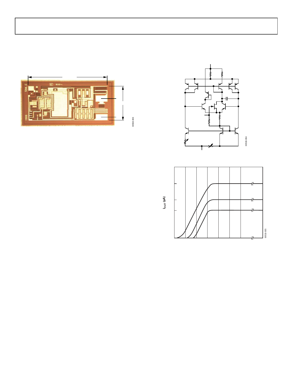
66MILS
V+
42MILS
V–
PTAT current. Figure 4 is the schematic diagram of the AD590.
In this figure, Q8 and Q11 are the transistors that produce the
PTAT voltage. R5 and R6 convert the voltage to current. Q10,
whose collector current tracks the collector currents in Q9 and
Q11, supplies all the bias and substrate leakage current for the
rest of the circuit, forcing the total current to be PTAT. R5 and
R6 are laser-trimmed on the wafer to calibrate the device at
25°C.
Figure 5 shows the typical V–I characteristic of the circuit at
25°C and the temperature extremes.
+
R1
R2
260Ω 1040Ω
Q2
Q5
Q3
Q1
Q4
C1
Q6
26pF
Q7
Q12
Q8
CHIP
SUBSTRATE R3
5kΩ
R4
11kΩ
Q9
Q10
Q11
8
R6
820Ω
R5 1
146Ω
1
–
Figure 4. Schematic Diagram
+150°C
423
THE AD590 IS AVAILABLE IN LASER-TRIMMED CHIP FORM;
CONSULT THE CHIP CATALOG FOR DETAILS
Figure 3. Metalization Diagram
CIRCUIT DESCRIPTION1
The AD590 uses a fundamental property of the silicon
transistors from which it is made to realize its temperature
proportional characteristic: if two identical transistors are
operated at a constant ratio of collector current densities, r, then
the difference in their base-emitter voltage will be (kT/q)(In r).
Since both k (Boltzman’s constant) and q (the charge of an
electron) are constant, the resulting voltage is directly
proportional to absolute temperature (PTAT).
In the AD590, this PTAT voltage is converted to a PTAT current
by low temperature coefficient thin-film resistors. The total
current of the device is then forced to be a multiple of this
1 For a more detailed description, see M.P. Timko, “A Two-Terminal IC
Temperature Transducer,” IEEE J. Solid State Circuits, Vol. SC-11, p. 784-788,
Dec. 1976. Understanding the Specifications–AD590.
+25°C
298
–55°C
218
0
1
2
3
4
5
6
30
SUPPLY VOLTAGE (V)
Figure 5. V-1 Plot
EXPLANATION OF TEMPERATURE SENSOR
SPECIFICATIONS
The way in which the AD590 is specified makes it easy to apply
in a wide variety of applications. It is important to understand
the meaning of the various specifications and the effects of
supply voltage and thermal environment on accuracy.
Rev. C | Page 6 of 16
Share Link: 