LTC1443CN(RevA) 데이터 시트보기 (PDF) - Linear Technology
부품명
상세내역
제조사
LTC1443CN Datasheet PDF : 12 Pages
| |||
LTC1443/LTC1444/LTC1445
APPLICATIO S I FOR ATIO
Bypassing the reference can help prevent false tripping of
the comparators by preventing glitches on the V+ or the
reference output voltage. Figure 3 shows the bypassed
reference output with a square wave applied to the V+ pin.
Resistors R1 and R2 set 10mV of hysteresis, while R3
damps the reference response. Note that the comparator
output doesn’t trip.
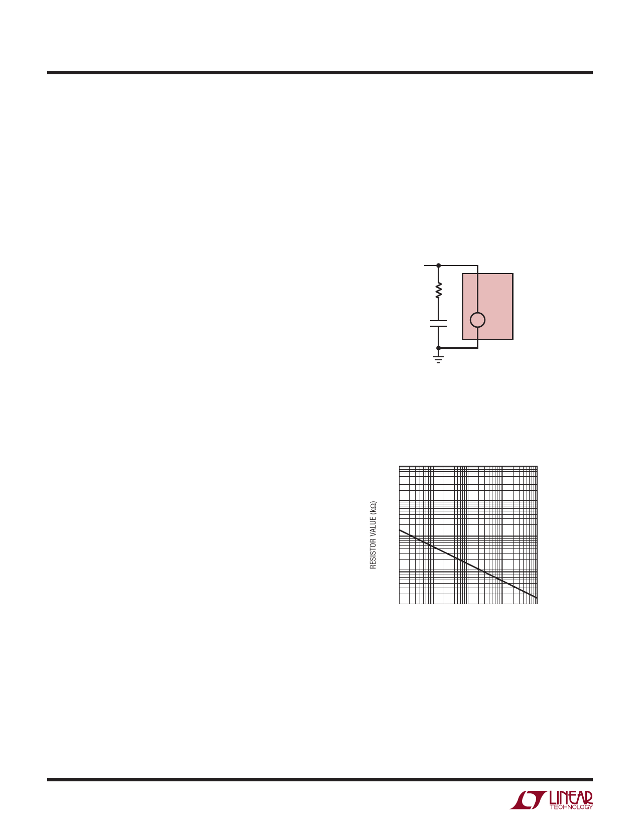
Hysteresis
Hysteresis can be added to the LTC1444/LTC1445 by
connecting a resistor (R1) between the REF and HYST
pins, and a second resistor (R2) from HYST to V – (Figure 4).
The difference between the upper and lower threshold volt-
ages or hysteresis voltage band (VHB) is equal to twice the
voltage difference between the REF and HYST pins. When
more hysteresis is added, the upper threshold increases the
same amount as the lower threshold decreases. The maxi-
mum voltage allowed between REF and HYST is 50mV,
producing a maximum hysteresis voltage band of 100mV. If
hysteresis is not wanted, the HYST pin should be shorted to
REF. Acceptable values for IREF range from 0.1µA to 5µA. If
2.4M is chosen for R2, then R1(kΩ) = VHB (mV).
5V
TO 8V
R1
10k
R2
2.4M
3
V+
5 IN A+ +
4 IN A– –
2
OUT
14 HYST
8 REF
LTC1445
R3
430Ω
C1
1.0µF
V–
9
LTC1443/44/45 • F03
Figure 3a. V + Glitching Test Circuit
8V
V+
5V
VREF
OUT
2ms/DIV
LTC1443/1444/1445 • TA02
Figure 3b. V + Glitching Response
8
IREF
R1
8
REF
LTC1445
14 HYST
R2
9
R1 = VHB
(2)(IREF)
( ) 1.221V – VHB
2
R2 =
IREF
LTC1443/44/45 • F04
Figure 4. Programmable Hysteresis
Share Link: 