CMX654D4 데이터 시트보기 (PDF) - MX-COM Inc
부품명
상세내역
제조사
CMX654D4 Datasheet PDF : 12 Pages
| |||
V.23 Transmit Modulator
10
CMX654 PRELIMINARY INFORMATION
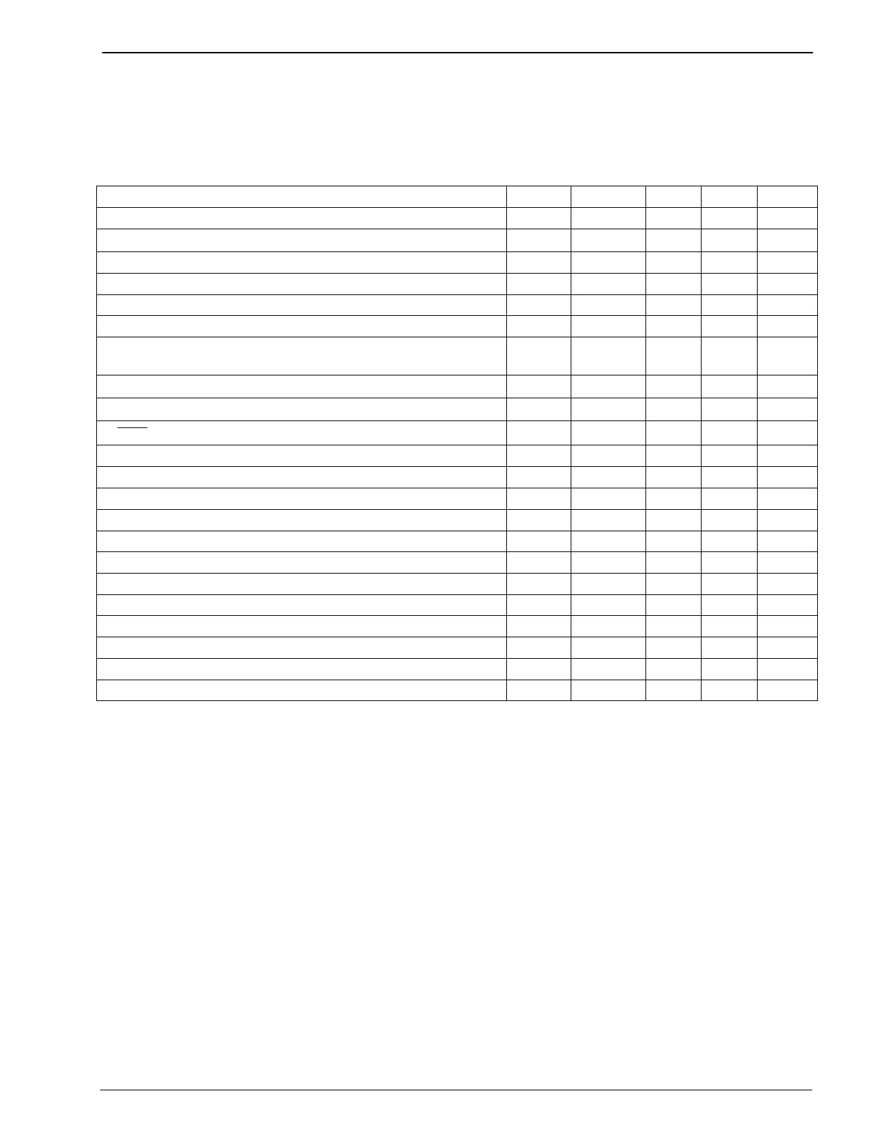
6.1.3 Operating Characteristics
For the following conditions unless otherwise specified:
VDD = 3.0V at TAMB = 25°C and VDD = 3.3V to 5.5V at TAMB = -40 to +85°C,
Xtal Frequency = 3.579545MHz r 0.1%, 0dBV corresponds to 1.0VRMS ,
0dBm corresponds to 775mVRMS into 600:.
DC Parameters
IDD (M0='1', M1='1')
IDD (M0 or M1='0') at VDD = 3.0V
IDD (M0 or M1='0') at VDD= 5.0V
Logic '1' Input Level
Logic '0' Input Level
Logic Input Leakage Current (VIN = 0 to VDD), Excluding
XTAL/CLOCK Input
Output Logic '1' Level (lOH = 360PA)
Output Logic '0' Level (lOL = -360PA)
RDY Output 'off' State Current (VOUT = VDD)
FSK Retiming
Tx Data Rate
FSK Modulator
TXOUT Level
Twist (Mark Level WRT Space Level)
Tx 1200bits/sec (M1='0', M0='1').
Bit Rate
Mark (Logical 1) Frequency
Space (Logical 0) Frequency
XTAL/CLOCK Input
'High' Pulse Width
'Low' Pulse Width
Notes Min.
1, 2
1
1
70%
-1.0
VDD-0.4
1194
3
-1.0
-2.0
0
1297
2097
4
100
4
100
Typ.
1
1.0
1.7
0
0
1200
Max.
1.25
2.5
30%
1.0
0.4
1.0
1206
1.0
2.0
1212
1303
2103
Units
PA
mA
mA
VDD
VDD
PA
V
V
PA
Baud
dB
dB
Baud
Hz
Hz
ns
ns
Operating Characteristics Notes:
1. At 25qC, not including any current drawn from the CMX654 pins by external circuitry other than X1, C1
and C2.
2. TXD and CLK inputs at VSS, M0 and M1 inputs at VDD.
3. Relative to 775mVRMS at VDD= 5.0V for load resistance greater than 40k:.
4. Timing for an external input to the XTAL/CLOCK pin.
¤1998 MX-COM, Inc.
www.mxcom.com Tel: 800 638 5577 336 744 5050 Fax: 336 744 5054
Doc. # 20480186.001
4800 Bethania Station Road, Winston-Salem, NC 27105-1201 USA All Trademarks and Service marks are held by their respective companies.
Share Link: 