CMX654D4 데이터 시트보기 (PDF) - MX-COM Inc
부품명
상세내역
제조사
CMX654D4 Datasheet PDF : 12 Pages
| |||
V.23 Transmit Modulator
6
CMX654 PRELIMINARY INFORMATION
4 General Description
4.1 Xtal Oscillator and Clock Dividers
Frequency and timing accuracy of the CMX654 is determined by a 3.579545MHz clock present at the
XTAL/CLOCK pin. This may be generated by the on-chip oscillator inverter using the external components
C1, C2 and X1 of Figure 2, or may be supplied from an external source to the XTAL/CLOCK input. If supplied
from an external source, C1, C2 and X1 should not be fitted.
The on-chip oscillator is turned off in the 'Zero-Power' mode.
If the clock is provided by an external source, which is not always running, then the 'Zero-Power' mode must
be set when the clock is not available. Failure to observe this rule may cause a significant rise in the supply
current drawn by CMX654 as well as generating undefined states of the RDY output.
4.2 Mode Control Logic
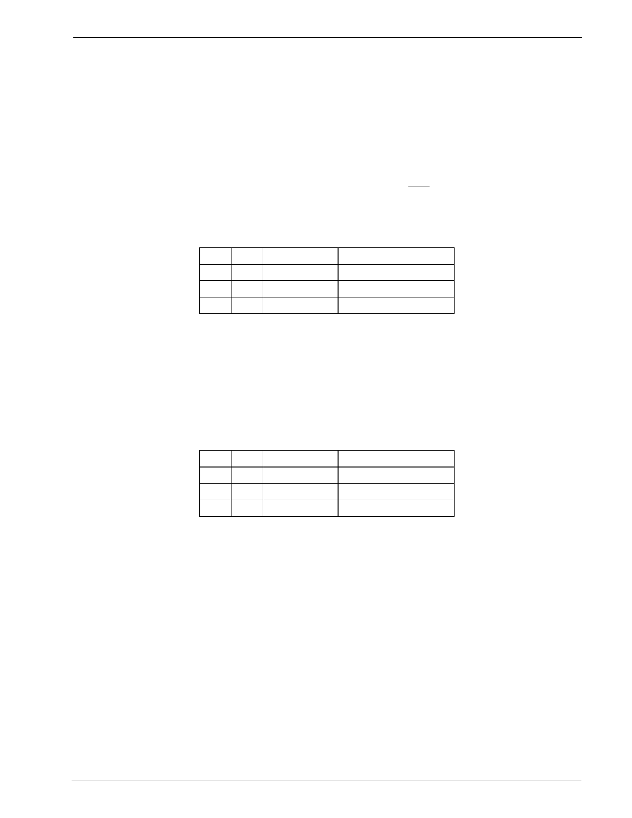
The CMX654's operating mode is determined by the logic levels applied to the M0 and M1 input pins:
M1 M0 Tx Mode
0 1 1200bits/sec
10
off
1 1 'Zero-Power'
[1] If enabled
Data Retime[1]
Tx
-
-
In the 'Zero-Power' mode, power is removed from all internal circuitry. When leaving 'Zero-Power' mode there
must be a delay of 20ms before any Tx data is passed to the device to allow the bias level, filters and
oscillator to stabilize. On applying power to the device the mode must be set to 'ZP', i.e. M0=1, M1=1, until
VDD has stabilized.
4.3 FSK Modulator and Transmit Filter
These blocks produce a tone according to the TXD, M0 and M1 inputs as shown in the table below, assuming
data retiming is not being used:
M1 M0 TXD = '0'
TXD = '1'
1 1 ‘Zero Power’
‘Zero Power’
10
0Hz
0Hz[1]
01
2100Hz
1300Hz
[1] TXOUT held at approx. VDD/2.
When modulated at the appropriate baud rates, the Transmit Filter and associated external components (see
Section 5.1) limit the FSK out of band energy sent to the line in accordance with Figure 3 assuming that the
signal on the line is at -6dBm or less.
¤1998 MX-COM, Inc.
www.mxcom.com Tel: 800 638 5577 336 744 5050 Fax: 336 744 5054
Doc. # 20480186.001
4800 Bethania Station Road, Winston-Salem, NC 27105-1201 USA All Trademarks and Service marks are held by their respective companies.
Share Link: 