ECP200G 데이터 시트보기 (PDF) - Unspecified
부품명
상세내역
제조사
ECP200G Datasheet PDF : 7 Pages
| |||
AH312
2 Watt, High Linearity InGaP HBT Amplifier
The Communications Edge TM
Product Information
Product Features
Product Description
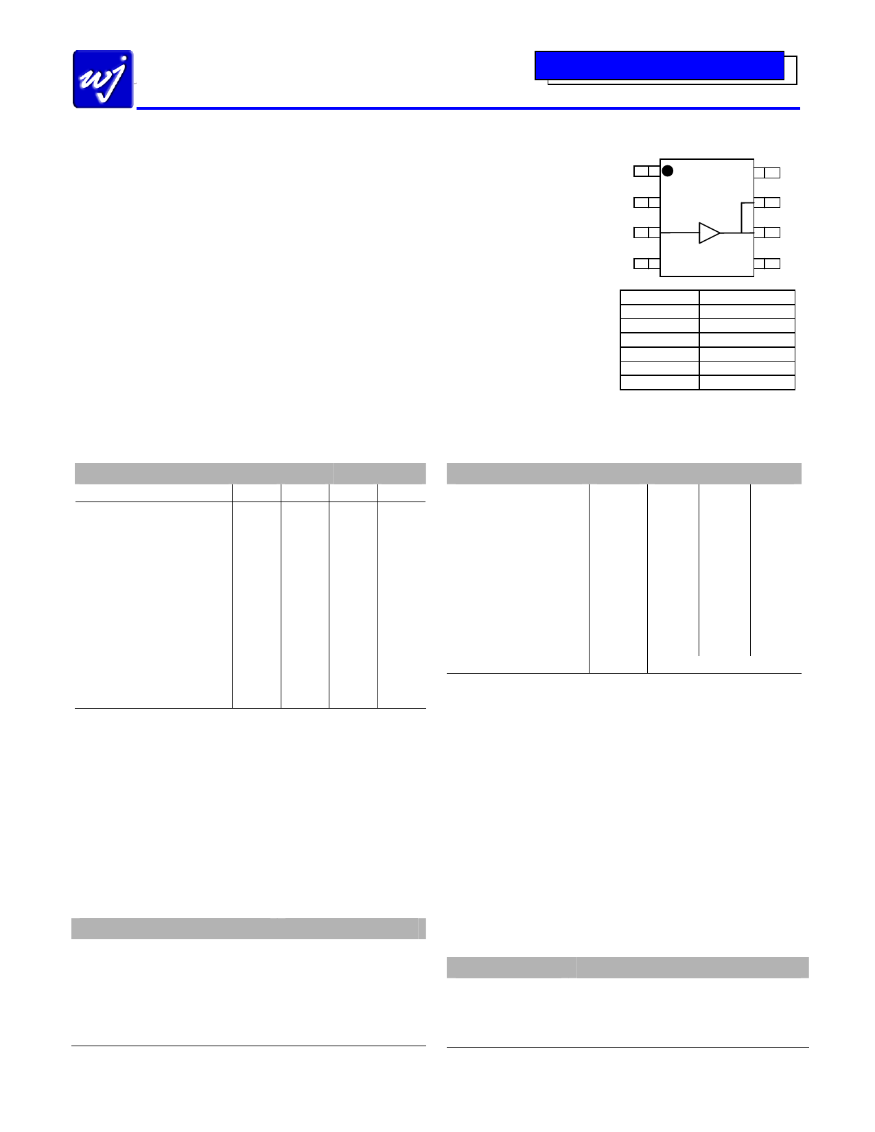
Functional Diagram
• 400 – 2300 MHz
• +33 dBm P1dB
• +51 dBm Output IP3
• 18 dB Gain @ 900 MHz
• +5V Single Positive Supply
The AH312 is a high dynamic range driver amplifier in a
low-cost surface mount package. The InGaP/GaAs HBT is
able to achieve high performance for various narrowband-
tuned application circuits with up to +49 dBm OIP3 and
+33 dBm of compressed 1dB power. It is housed in a lead-
free/green/RoHS-compliant SOIC-8 package. All devices are
100% RF and DC tested.
• MTTF > 100 Years
• Lead-free/green/RoHS-compliant
SOIC-8 SMT Pkg.
Applications
• Final stage amplifiers for Repeaters
• Mobile Infrastructure
The AH312 is targeted for use as a driver amplifier in
wireless infrastructure where high linearity and medium
power is required. An internal active bias allows the
AH312 to maintain high linearity over temperature and
operate directly off a single +5V supply. This combination
makes the device an excellent candidate for transceiver line
cards in current and next generation multi-carrier 3G base
stations.
1
8
2
7
3
6
4
5
Function
Vref
Input
Output
Vbias
GND
N/C or GND
Pin No.
1
3
6, 7
8
Backside Paddle
2, 4, 5
Specifications (1)
Typical Performance (4)
Parameter
Units
Operational Bandwidth
MHz
Test Frequency
MHz
Gain
dB
Input R.L.
dB
Output R.L.
dB
Output P1dB
Output IP3 (2)
dBm
dBm
IS-95A Channel Power
@ -45 dBc ACPR, 1960 MHz
wCDMA Channel Power
@ -45 dBc ACLR, 2140 MHz
Noise Figure
Operating Current Range, Icc (3)
dBm
dBm
dB
mA
Device Voltage, Vcc
V
Min
400
9
+32
+47
700
Typ
2140
10
20
6.8
+33.2
+48
+27.5
+25.3
7.7
800
+5
Max
2300
900
1. Test conditions unless otherwise noted: 25ºC, +5V Vsupply, 2140 MHz, in tuned application circuit.
2. 3OIP measured with two tones at an output power of +17 dBm/tone separated by 1 MHz. The
suppression on the largest IM3 product is used to calculate the 3OIP using a 2:1 rule.
3. This corresponds to the quiescent current or operating current under small-signal conditions into
pins 6, 7, and 8. It is expected that the current can increase by an additional 200 mA at P1dB. Pin
1 is used as a reference voltage for the internal biasing circuitry. It is expected that Pin 1 will pull
22mA of current when used with a series bias resistor of R1=15Ω. (ie. total device current
typically will be 822 mA.)
Parameter
Frequency
S21 – Gain
S11 – Input R.L.
S22 – Output R.L.
Output P1dB
Output IP3
IS-95A Channel Power
@ -45 dBc ACPR
wCDMA Channel Power
@ -45 dBc ACLR
Noise Figure
Device Bias (3)
Units
MHz
dB
dB
dB
dBm
dBm
dBm
dBm
dB
Typical
900 1960 2140
18
11
10
-18
-19
-20
-11 -6.8 -6.8
+33 +33.4 +33.2
+49 +51 +48
+27 +27.5
+25.3
8.0
7.3
7.7
+5 V @ 800 mA
4. Typical parameters reflect performance in a tuned application circuit at +25° C.
Absolute Maximum Rating
Parameter
Operating Case Temperature
Storage Temperature
RF Input Power (continuous)
Device Voltage
Device Current
Device Power
Junction Temperature
Rating
-40 to +85 °C
-65 to +150 °C
+28 dBm
+8 V
1400 mA
8W
+250 °C
Ordering Information
Part No.
AH312-S8G
AH312-S8PCB900
AH312-S8PCB1960
AH312-S8PCB2140
Description
2 Watt, High Linearity InGaP HBT Amplifier
(lead-free/green/RoHS-compliant SOIC-8 Pkg)
900 MHz Evaluation Board
1960 MHz Evaluation Board
2140 MHz Evaluation Board
Operation of this device above any of these parameters may cause permanent damage.
Specifications and information are subject to change without notice.
WJ Communications, Inc • Phone 1-800-WJ1-4401 • FAX: 408-577-6621 • e-mail: sales@wj.com • Web site: www.wj.com
Page 1 of 7 March 2006
Share Link: 